Semiconductor device in which semiconductor chip is mounted on lead frame
a semiconductor chip and lead frame technology, applied in semiconductor devices, semiconductor/solid-state device details, electrical equipment, etc., can solve the problems of inability to meet the requirements of the above-described lead frame, the lead frame is not versatile in packaging, and the adjacent bonding wire is likely to undergo short-circuiting
- Summary
- Abstract
- Description
- Claims
- Application Information
AI Technical Summary
Problems solved by technology
Method used
Image

Examples
first embodiment
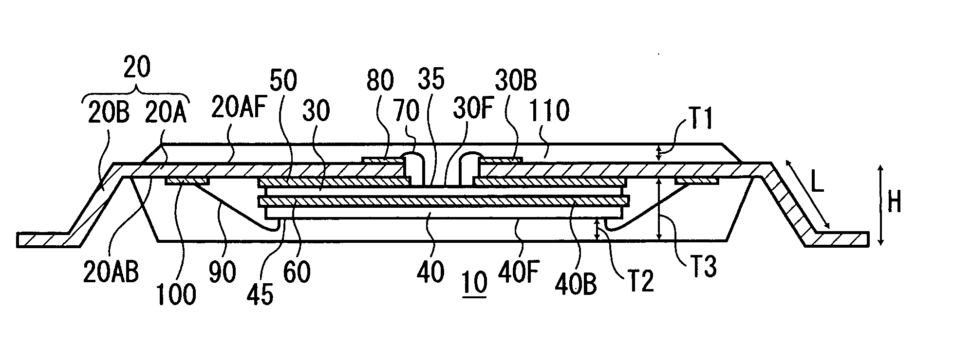
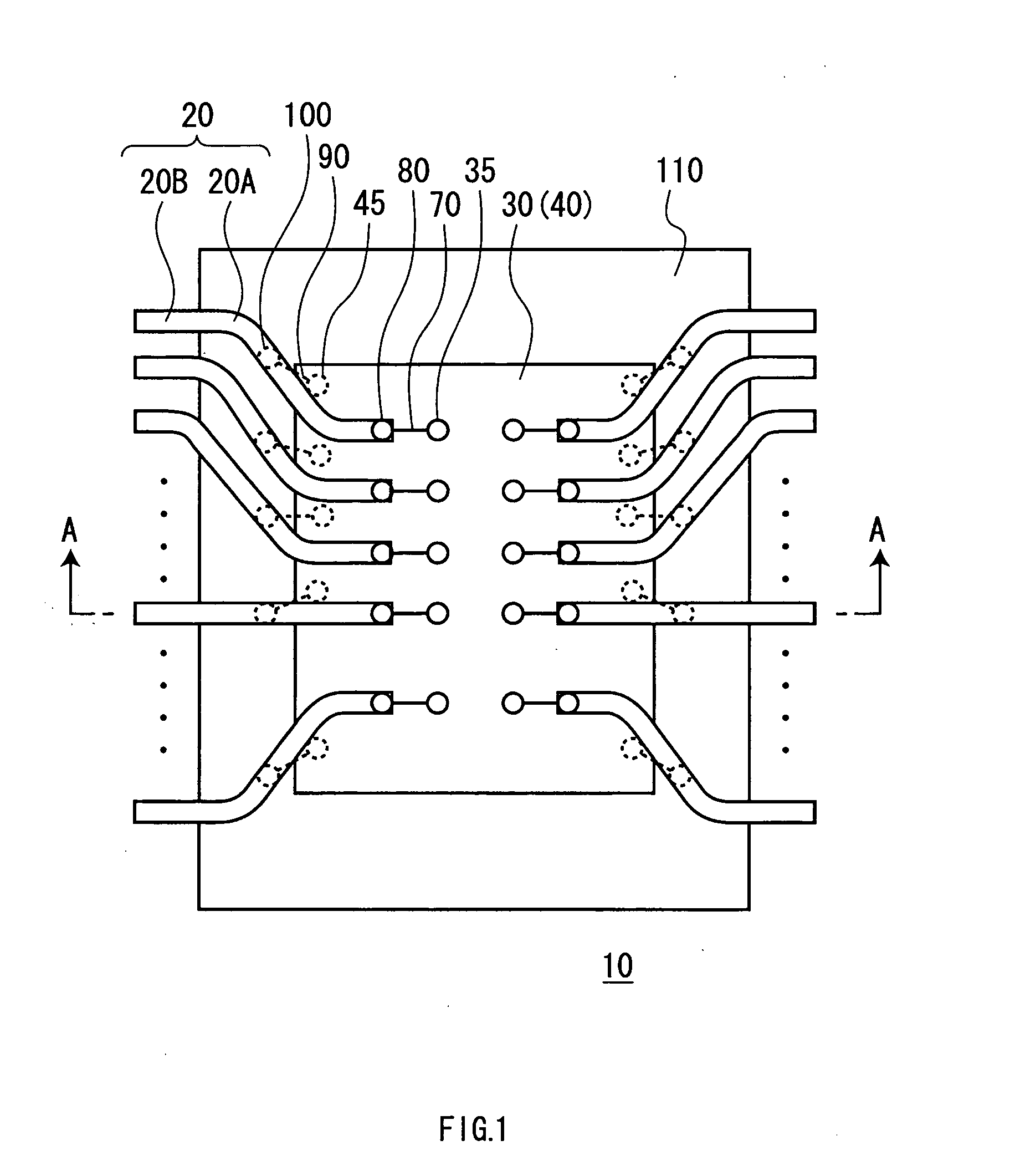
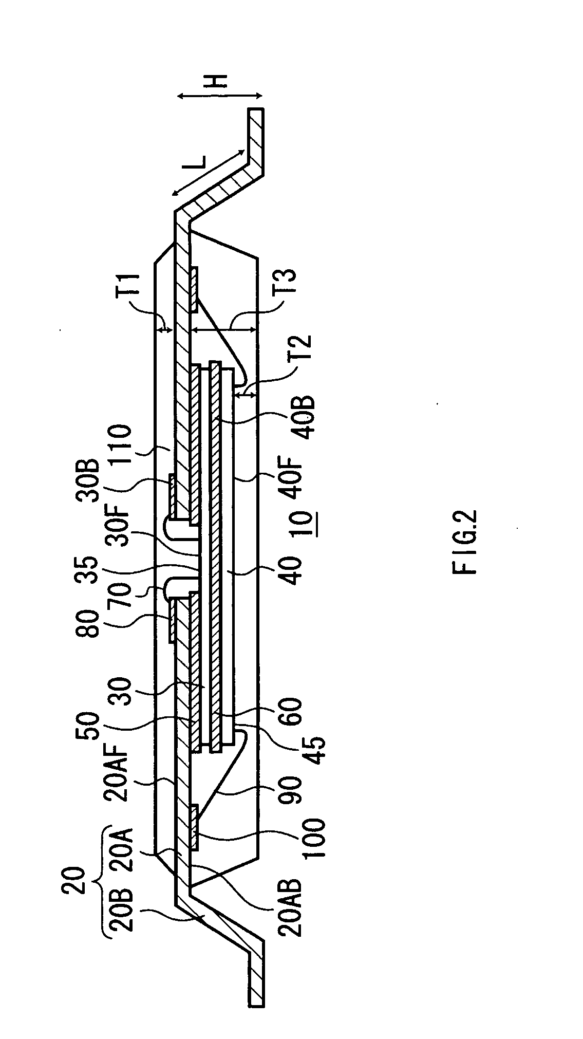
[0018] Referring now to the drawings, wherein like reference numerals designate identical or corresponding parts throughout the several views, and more particularly to FIG. 1 thereof, FIG. 1 shows the semiconductor device 10 according to a FIG. 2 shows a sectional view of the semiconductor device 10 along A-A line in FIG. 1. An LOC (Lead On Chip) structure in which a semiconductor chip is mounted on lower surfaces (hereinafter referred to as “back surfaces”) of inner leads is used for the semiconductor device 10 for the purpose of making package size small.
[0019] The lead frame 20 has inner leads 20A and outer leads 20B. The inner leads 20A are located inside a package 110. The inner leads 20A are electrically connected to bonding pads 35 and 45. The bonding pads 35 are arranged on a first semiconductor chip 30 and the bonding pads 45 are arranged on a second semiconductor chip 40, respectively. The outer leads 20B are integrated with inner leads 20A.
[0020] Insulating die bond tap...
second embodiment
[0034]FIG. 3 shows the semiconductor device 200 according to a The semiconductor chip 210 of which bonding pads (not shown) are arranged on a peripheral region of an element formation surface 210F is shown in FIG. 3. The semiconductor chip 210 is adhered to end portions of back surfaces 20AB of the inner leads 20A with the insulating die bond tapes 50, in a state where the element formation surface 210F of the semiconductor chip 210 is turned down.
[0035] Second plating 100 is provided on the back surfaces 20AB of the inner leads 20A. The bonding pads of the semiconductor chip 210 are electrically connected to the second plating 100 by second bonding wires 90.
[0036] According to the second embodiment, the same lead frame 20 as the first embodiment can be used. Therefore, the versatility on packaging can be raised.
third embodiment
[0037] Next, FIG. 4 shows the semiconductor device 300 according to a The semiconductor chip 310 of which bonding pads (not shown) are arranged on a central region of an element formation surface 310F is shown in FIG. 4. The semiconductor chip 310 is adhered to end portions of back surfaces 20AB of the inner leads 20A with the insulating die bond tapes 50, in a state where the element formation surface 310F of the semiconductor chip 310 is turned up.
[0038] First plating 80 is provided at end portions of front surfaces 20AF of the inner leads 20A. The bonding pads of the semiconductor chip 310 are electrically connected to the first plating 80 by first bonding wires 70.
[0039] According to the third embodiment, the same lead frame 20 as the first embodiments can be used, as well as the second embodiment. Therefore, the versatility on packaging can be raised.
PUM
 Abstract
Description
Claims
Application Information
 - Generate Ideas
- Intellectual Property
- Life Sciences
- Materials
- Tech Scout
- Unparalleled Data Quality
- Higher Quality Content
- 60% Fewer Hallucinations
Browse by: Latest US Patents, China's latest patents, Technical Efficacy Thesaurus, Application Domain, Technology Topic, Popular Technical Reports.
© 2025 PatSnap. All rights reserved.Legal|Privacy policy|Modern Slavery Act Transparency Statement|Sitemap|About US| Contact US: help@patsnap.com