SiC material, semiconductor device fabricating system and SiC material forming method
a technology of semiconductor devices and forming methods, applied in the direction of crystal growth process, polycrystalline material growth, chemically reactive gases, etc., can solve the problems of reducing the life of parts, reducing the efficiency of film forming, and reducing the efficiency of wet cleaning, so as to achieve excellent corrosion resistance and uniform surface
- Summary
- Abstract
- Description
- Claims
- Application Information
AI Technical Summary
Benefits of technology
Problems solved by technology
Method used
Image

Examples
first embodiment
[0051] A highly corrosion-resistant SiC material in a first embodiment of the present invention will be described. The SiC material contains β-SiC crystals and is formed by a CVD process (chemical vapor deposition process).
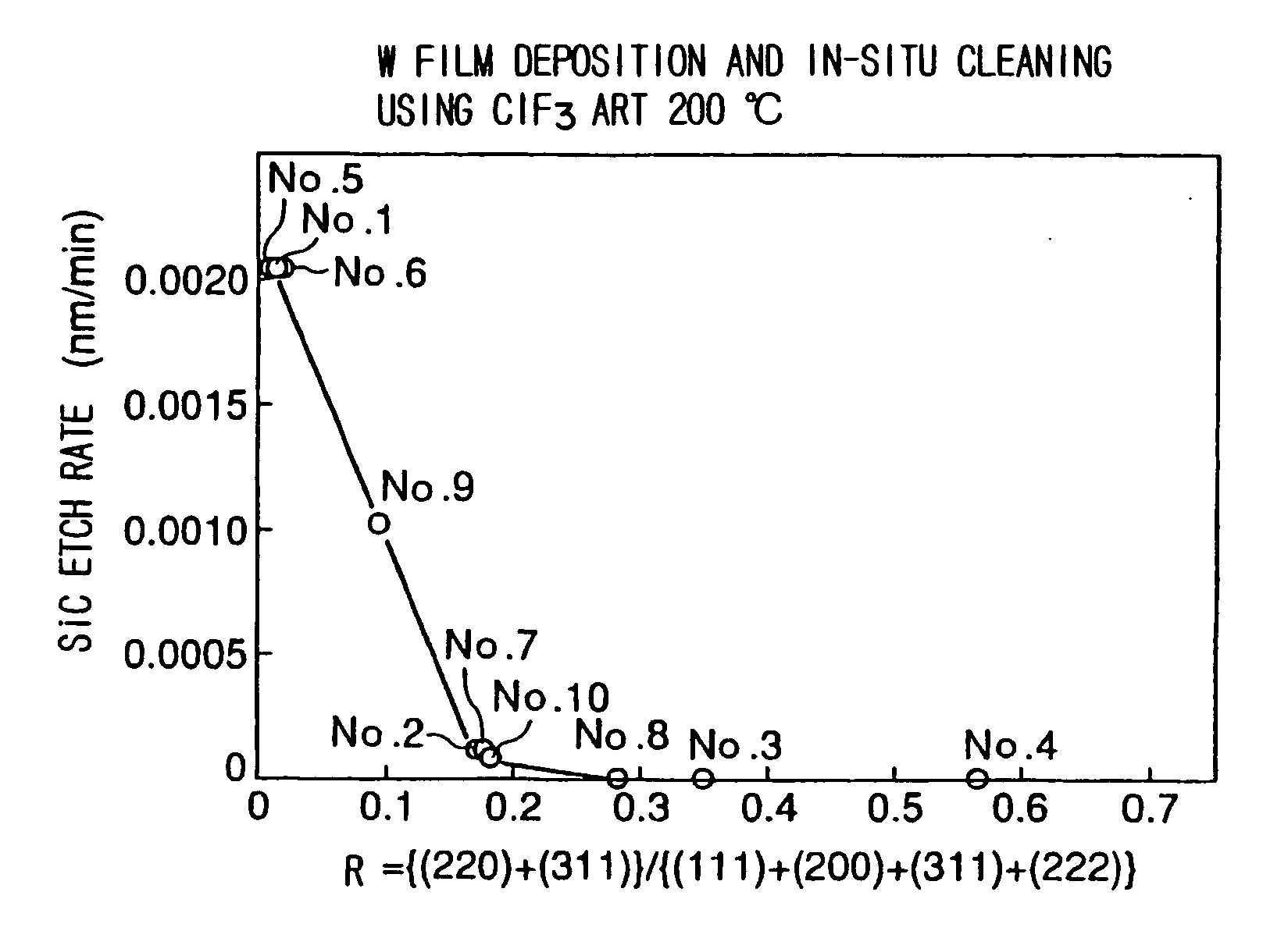
[0052] The SiC material formed by the CVD process (hereinafter referred to also as “CVD-SiC material”) contains β-SiC crystals oriented such that the ratio of the sum of the respective peak intensities of x-ray diffraction for (220) and (311) planes of the β-SiC crystals to the sum of the respective peak intensities of x-ray diffraction for (111), (200), (220), (311) and (222) planes of the β-SiC crystals is 0.15 or above. SiC crystals are classified largely into α-SiC crystals, i.e., hexagonal crystals, and β-SiC crystals, i.e., cubic crystals. As generally known, β-SiC crystals are more excellent than α-SiC crystals in high-temperature chemical stability. A part, such as a susceptor, formed by coating a base body with a β-SiC material has been employed in a CVD...
second embodiment
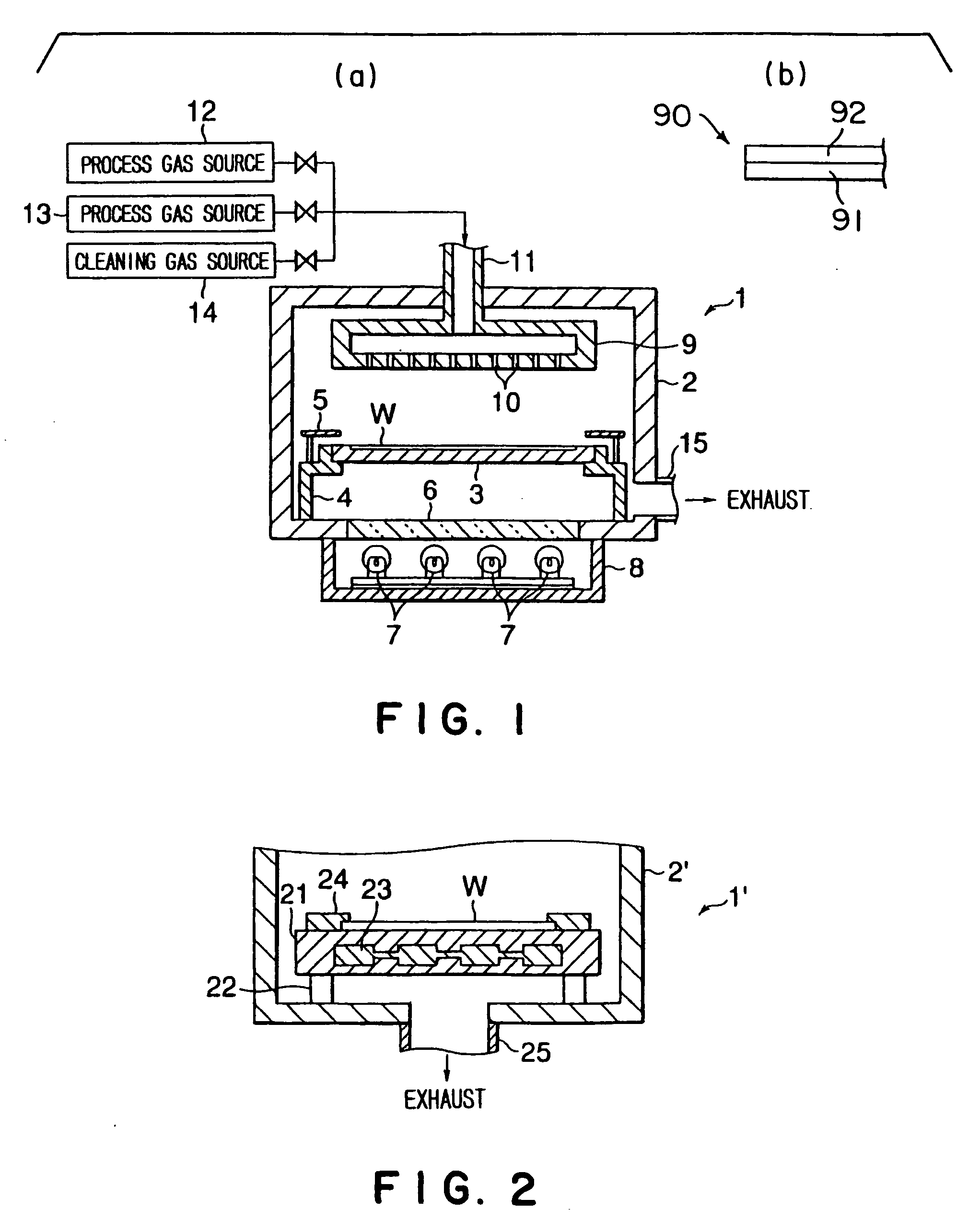
[0091] A second embodiment of the present invention will be described with reference to FIGS. 11 to 15. FIGS. 11 to 15 show different semiconductor device fabricating systems each provided with internal component parts analogous to the internal component member 90 formed by coating the base body 91 with the CVD-SiC material 92 in the first embodiment of the present invention. The internal component member 90 consisting of the base body 91 and the SiC material 92 can be used not only in the CVD system mentioned in the description of the first embodiment, but also in other CVD systems, such as a plasma CVD system.
[0092] Naturally, the internal component member 90 consisting of the base body 91 and the SiC material 92 is applicable to not only a CVD system using a halogen-containing gas as a cleaning gas, but also a dry-etching system using a halogen-containing gas as a process gas.
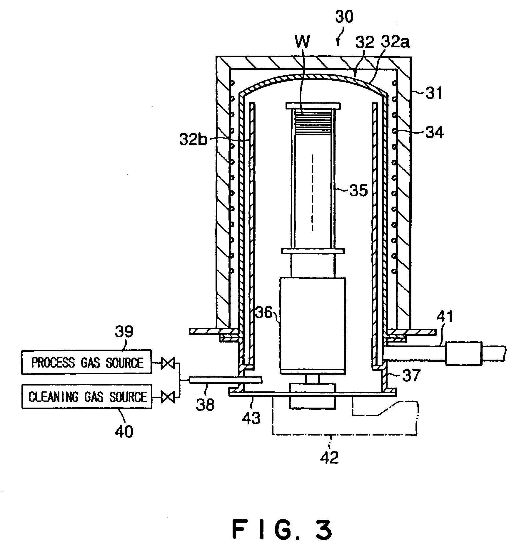
[0093] An etching system provided with an internal component member coated with the CVD-SiC material of...
examples
[0112] The relation between R-value and etch rate when test pieces are exposed to a plasma in a plasma etching system will be described.
[0113] Samples of internal members in Examples 1 to 8 coated with the CVD-SiC material and an internal member of Al2O3 in Comparative example were prepared. The samples were subjected to the following etching experiment.
[0114] (1) Conditions for Experiment [0115] System; TE8500S ESC 8″[0116] Time; 20 hr [0117] n: 1 or 2 [0118] Process conditions[0119] Power; 1300 W, Pressure: 1000 mT, CF4 / Ar=02 / 95=950 [0120] sccm / 10 sccm [0121] Size of sample: 20 Sq. mm×2 mm thickness or 30 mm diameter×2 mm thickness [0122] Quality of sample: CVD-SiC (R=0.0004 to 0.561) [0123] Base body: Porous SiC, graphite, CVD-SiC material.
[0124] Method of evaluation: The surface of each sample excluding a central region of 10 sq. mm was masked with a mask M of Kapton tape as shown in FIG. 16. Samples were attached to parts of a 8 inch wafer on concentric circles with a double...
PUM
| Property | Measurement | Unit |
|---|---|---|
| temperature | aaaaa | aaaaa |
| size | aaaaa | aaaaa |
| thick | aaaaa | aaaaa |
Abstract
Description
Claims
Application Information
 - R&D
- Intellectual Property
- Life Sciences
- Materials
- Tech Scout
- Unparalleled Data Quality
- Higher Quality Content
- 60% Fewer Hallucinations
Browse by: Latest US Patents, China's latest patents, Technical Efficacy Thesaurus, Application Domain, Technology Topic, Popular Technical Reports.
© 2025 PatSnap. All rights reserved.Legal|Privacy policy|Modern Slavery Act Transparency Statement|Sitemap|About US| Contact US: help@patsnap.com