Method of manufacturing semiconductor device
a semiconductor and semiconductor technology, applied in the direction of semiconductor devices, basic electric elements, electrical equipment, etc., can solve the problems of serious degradation of refresh characteristics in dram, cell transistor characteristics degrade where they are formed, etc., and achieve good characteristics
- Summary
- Abstract
- Description
- Claims
- Application Information
AI Technical Summary
Benefits of technology
Problems solved by technology
Method used
Image

Examples
first embodiment
[0041]FIG. 1 to FIG. 11 are schematic sectional views showing manufacturing processes of DRAM according to the present invention.
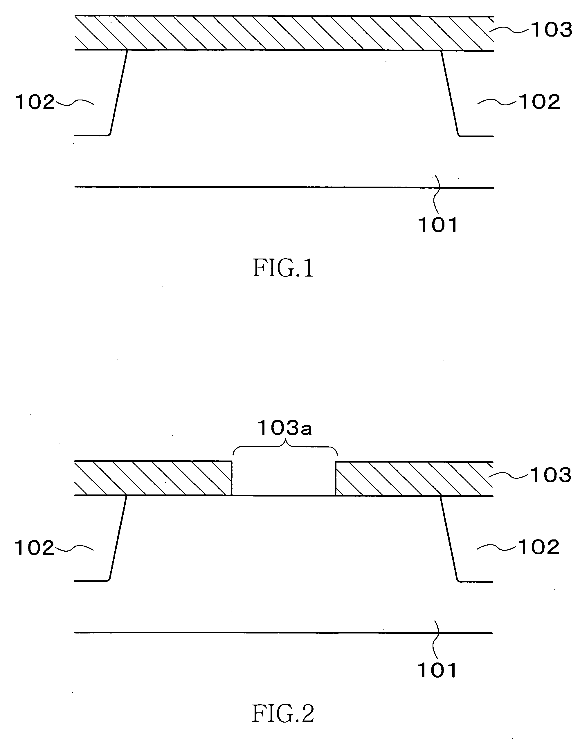
[0042] First, as shown in FIG. 1, in the manufacturing of DRAM, element isolation regions 102 having a depth of approximately 250 to 350 nm are formed on the surface of a P-type silicon substrate 101 by a STI method. After that, a silicon nitride film 103 having approximately 100 to 200 nm is deposited on the surface of the P-type silicon substrate 101 by a CVD method.
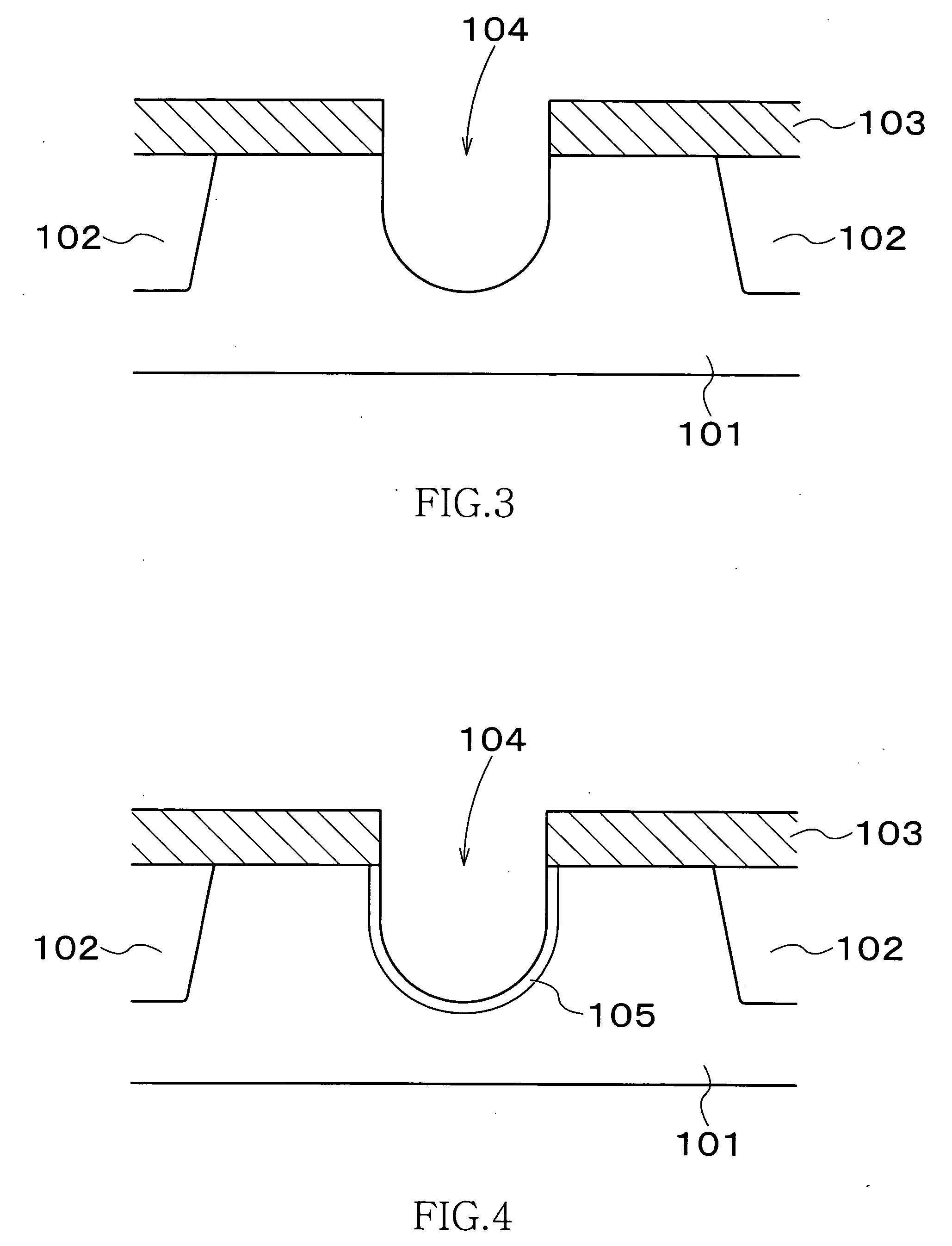
[0043] Next, as shown in FIG. 2, the silicon nitride film 103 is selectively eliminated by a photolithography technology, thereby forming an opening 103a of a predetermined pattern in the silicon nitride film 103. Then, the P-type silicon substrate 101 is subjected to dry etching using this silicon nitride film 103 as a mask, thereby forming a trench (gate trench) 104 having a depth of approximately 100 to 200 nm in a predetermined region to be formed by a channel region (a gate electrode), ...
second embodiment
[0051]FIG. 12 to FIG. 14 are schematic sectional views for schematically showing a part of manufacturing process of DRAM according to the present invention.
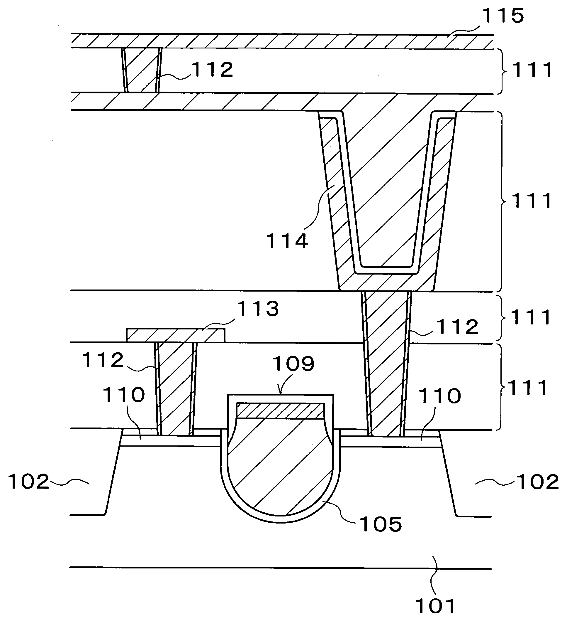
[0052] In the present embodiment, a sequence of process until a gate oxide film 105 is formed by forming a gate trench 104 on a P-type silicon substrate 101, is the same as the process of the first embodiment shown in FIG. 1 to FIG. 4; however, as shown in FIG. 12, a different point from the first embodiment is that a polycrystalline silicon film 106 is comparatively thinly formed so that a concave part 106X with the polycrystalline silicon film 106 is formed inside the gate trench 104. By thinly forming the polycrystalline silicon film 106, the inside of the gate trench 104 is not completely embedded with the polycrystalline silicon film 106; consequently, it becomes a state where the concave part 106X with the polycrystalline silicon film 106 is formed. Then, in this state, a silicide film 116 is deposited on the entire surface...
third embodiment
[0057]FIG. 15 is a schematic sectional view for schematically showing a part of manufacturing process of DRAM according to the present invention.
[0058] As shown in FIG. 15, in the present embodiment, a tungsten nitride film (WN) 117 and a tungsten film (W) 118 are sequentially deposited to form a polymetal gate electrode in a gate trench 104, in place of the silicide film 116 shown in FIG. 12 in the second embodiment. After that, the tungsten film 118, nitride tungsten film 117, and a polycrystalline silicon film 106 are polished by a CMP method until an upper surface of a silicon nitride film 103 is exposed so that these remain inside the gate trench 104 and within the opening of the silicon nitride film 103.
[0059] After that, a trench gate type transistor of the present embodiment is completed by eliminating the silicon nitride film 103, reinforcing a gate oxide film 105 by selective oxidation under Wet-Hydrogen atmosphere, and forming an N type diffusion layer 110 which becomes ...
PUM
| Property | Measurement | Unit |
|---|---|---|
| length | aaaaa | aaaaa |
| depth | aaaaa | aaaaa |
| depth | aaaaa | aaaaa |
Abstract
Description
Claims
Application Information
 - R&D
- Intellectual Property
- Life Sciences
- Materials
- Tech Scout
- Unparalleled Data Quality
- Higher Quality Content
- 60% Fewer Hallucinations
Browse by: Latest US Patents, China's latest patents, Technical Efficacy Thesaurus, Application Domain, Technology Topic, Popular Technical Reports.
© 2025 PatSnap. All rights reserved.Legal|Privacy policy|Modern Slavery Act Transparency Statement|Sitemap|About US| Contact US: help@patsnap.com