Liquid crystal display panel and method of fabricating the same

Active Publication Date: 2006-06-29
LG DISPLAY CO LTD
View PDF13 Cites 50 Cited by
  • Summary
  • Abstract
  • Description
  • Claims
  • Application Information

AI Technical Summary

Benefits of technology

[0011] An advantage of the present invention is to provide a liquid crystal display panel that is adaptive for being miniaturized as well as reducing a process time, and a fabricating method thereof.
[0012] Additional features and advantages of the invention will be set forth in the description which follows, and in part will be apparent from the description, or may be learned by practice of the invention. The objectives and other advantages of the invention will be realized and attained by the structure particularly pointed out in the written description and claims hereof as well as the appended drawings.
[0013] To achieve these and other advantages and in accordance with the purpose of the present invention, as embodied and broadly described, a liquid crystal display panel, including: a first substrate having a common electrode; a second substrate including a pixel electrode that forms an electric field with the common electrode, a thin film transistor connected to the pixel electrode, a signal line that applies a signal to the thin film transistor, and a contact area in an area outside an area where the signal line is, and the contact area applies a common voltage to the common electrode; and a sealant formed between the first and second substrates with a conductive spacer that connects the contact area with the common electrode.
[0014] In another aspect of the present invention, a liquid cry

Problems solved by technology

There is a problem in that the common voltage is distorted and a horizontal cross talk is generated because the line resistance of the common line is high.
In addition, for small liquid crystal display panels, the silver dot process needs to be performed

Method used


Image

  • Liquid crystal display panel and method of fabricating the same
  • Liquid crystal display panel and method of fabricating the same
  • Liquid crystal display panel and method of fabricating the same

Examples


Embodiment Construction

[0026] Reference will now be made in detail to an embodiment of the present invention, example of which is illustrated in the accompanying drawings.

[0027] Hereinafter, the preferred embodiments of the present invention will be described in detail with reference to FIGS. 2 to 7F.

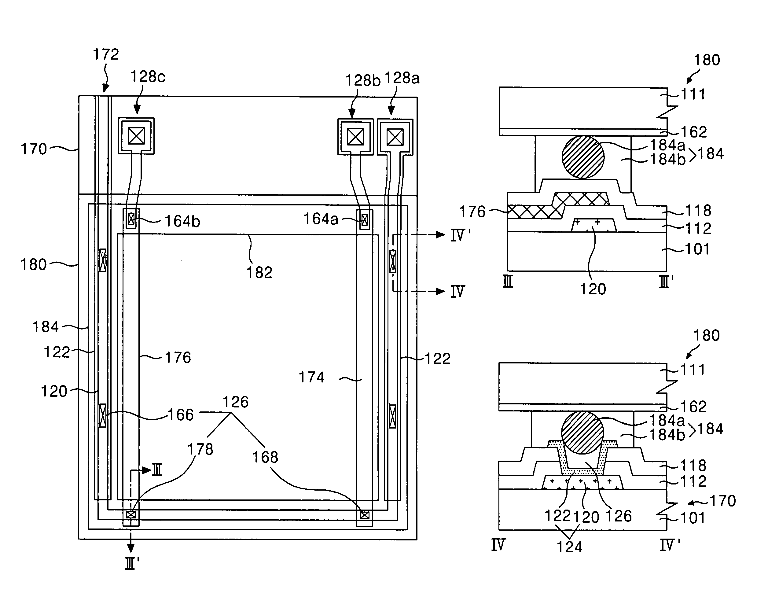
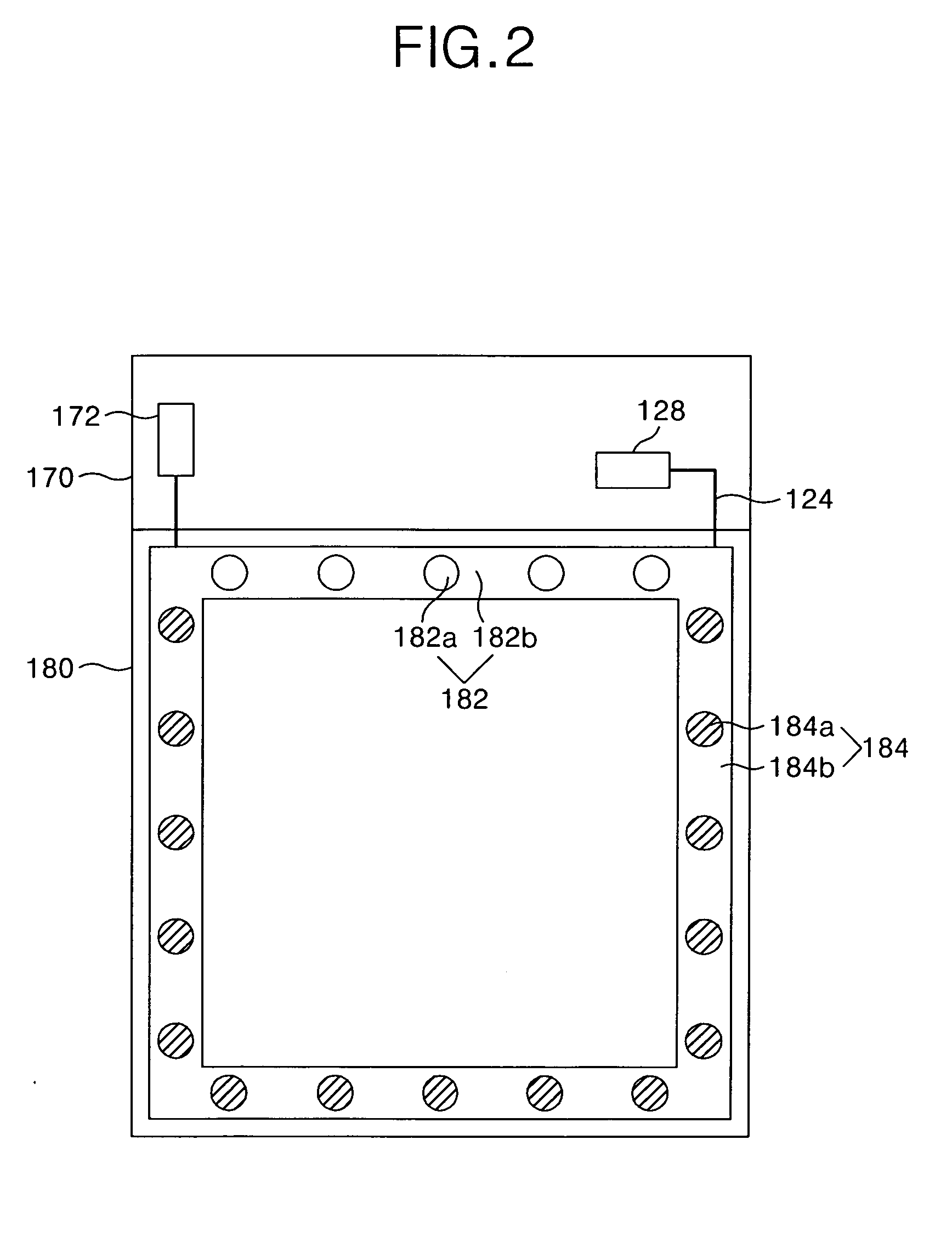
[0028]FIG. 2 is a plane view representing a liquid crystal display panel according to the first embodiment of the present invention.

[0029] Referring to FIG. 2, the liquid crystal display panel includes a thin film transistor array substrate 170 having a thin film transistor array; a color filter array substrate 180 having a color filter array; and a sealant 186 to bond the thin film transistor array substrate 170 and the color filter array substrate 180.

[0030] The thin film transistor array substrate 170 has a thin film transistor array that includes a gate line and a data line that cross each other, a thin film transistor at the crossing of the gate line and the data line, and a lower alignment film to a...


PUM


Abstract

This invention relates to a liquid crystal display panel, including: a first substrate having a common electrode; a second substrate including a pixel electrode that forms an electric field with the common electrode, a thin film transistor connected to the pixel electrode, a signal line that applies a signal to the thin film transistor, and a contact area in an area outside an area where the signal line is, and the contact area applies a common voltage to the common electrode; and a sealant formed between the first and second substrates with a conductive spacer that connects the contact area with the common electrode.

Description

[0001] This application claims the benefit of Korean Patent Application No. P2004-111511 filed on Dec. 23, 2004, which is hereby incorporated by reference for all purposes as if fully set forth herein. BACKGROUND OF THE INVENTION [0002] 1. Field of the Invention [0003] The present invention relates to a liquid crystal display panel and a fabricating method thereof, and more particularly to a miniaturized liquid crystal display panel as well as reducing the fabrication time thereof. [0004] 2. Description of the Related Art [0005] A liquid crystal display device controls the light transmissivity of liquid crystal by use of an electric field, thereby displaying a picture. The liquid crystal display device, as shown in FIG. 1, includes a thin film transistor array substrate 70 and a color filter array substrate 80 which are opposite to each other with a liquid crystal 16 therebetween. [0006] The thin film transistor array substrate 70 includes a gate line 2 and a data line 4 crossing ea...

Claims


Application Information

Patent Timeline
IPC IPC(8): G02F1/1339
CPCG02F1/13394G02F1/1343G02F1/1368G02F1/1339
Inventor AHN, BYUNG CHULLIM, JOO SOO
Owner LG DISPLAY CO LTD
Why Eureka
Try Eureka