Integrated circuit layout critical area determination using voronoi diagrams and shape biasing
a technology of voronoi diagrams and integrated circuits, applied in computer aided design, computation using non-denominational number representations, instruments, etc., can solve problems such as enlargement or shrinkage of intended printed shapes, defects that create open circuits, and shapes to print slightly smaller
- Summary
- Abstract
- Description
- Claims
- Application Information
AI Technical Summary
Problems solved by technology
Method used
Image
Examples
first embodiment
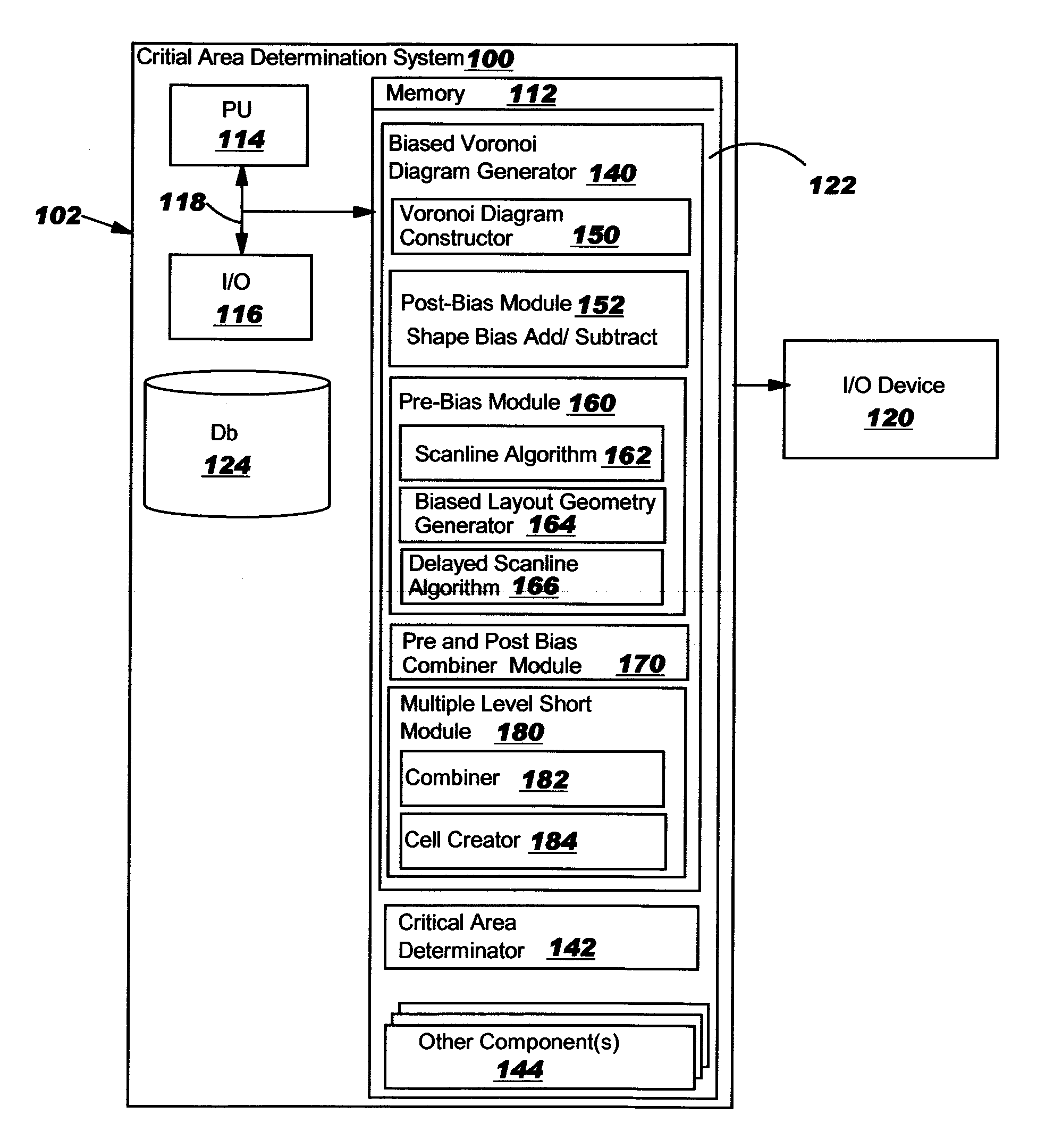
[0057]FIG. 8 illustrates a flow diagram of a method for generating a biased Voronoi diagram, referred herein as a “post-biasing” because the shape bias is incorporated into the Voronoi diagram after the diagram is generated. This embodiment requires application of a shape bias uniformly across all of the layout geometry.
[0058]FIG. 9 shows an illustration of two shapes 202, 204 (white background) of a simplified layout geometry 206 for used in describing this embodiment. Shapes 210, 212 (shaded) show a shape bias W1 of shapes 202, 204 causing an enlargement, respectively; and shapes 220, 222 (diagonal cross-hatching) show shape bias W1 causing a shrinkage of shapes 202, 204, respectively.
[0059] In a first step S100, Voronoi diagram constructor 150 (FIG. 6) constructs a preliminary Voronoi diagram of layout geometry 206 for modeling opens or shorts. That is, a Voronoi diagram is generated for layout geometry 206 in a conventional fashion according to whether the spot defects to be mo...
fourth embodiment
[0077]FIG. 14 shows a flow diagram of the invention for generating a biased Voronoi diagram and that addresses the situation where the layout geometry includes a plurality of regions in the form of levels, and each level includes a level shape bias particular to that level. This embodiment is implemented by multiple level short module 180 (FIG. 6), as will be described below. FIG. 15 shows a multiple level IC design 380 including multiple levels 390A, 390B, each with two overlapping shapes 392A, 392B for level 390A and 394A, 394B for level 390B.
[0078] In a first step S400, shown in FIGS. 14 and 16, each level 390A, 390B is pre-biased by pre-biasing module 160. In particular, in a first sub-step S400A, all levels of the layout geometry 380 are scanned by scanline algorithm 162 (FIG. 6) (see scanline 396 in FIG. 15). In one embodiment, all levels are scanned simultaneously. In a next sub-step S400B, a biased layout geometry is generated by biased layout geometry generator 164 (FIG. 6)...
PUM
 Abstract
Description
Claims
Application Information
 - R&D
- Intellectual Property
- Life Sciences
- Materials
- Tech Scout
- Unparalleled Data Quality
- Higher Quality Content
- 60% Fewer Hallucinations
Browse by: Latest US Patents, China's latest patents, Technical Efficacy Thesaurus, Application Domain, Technology Topic, Popular Technical Reports.
© 2025 PatSnap. All rights reserved.Legal|Privacy policy|Modern Slavery Act Transparency Statement|Sitemap|About US| Contact US: help@patsnap.com


