Check patentability & draft patents in minutes with Patsnap Eureka AI!

Vertical unipolar component

a technology of vertical unipolar components and components, applied in the manufacturing of semiconductor devices, semiconductor/solid-state devices, electric devices, etc., can solve the problems of complex structure and achieve the effect of high breakdown voltage and simple manufacturing structure of figs

Inactive Publication Date: 2006-09-14
STMICROELECTRONICS SRL
View PDF5 Cites 10 Cited by
  • Summary
  • Abstract
  • Description
  • Claims
  • Application Information

AI Technical Summary

Benefits of technology

The structure achieves improved breakdown voltage and reduced manufacturing complexity by optimizing equipotential surface distribution, enabling higher reverse breakdown voltages with minimal on-state resistance.

Problems solved by technology

However, such a structure is complex to manufacture.

Method used


Image

  • Vertical unipolar component
  • Vertical unipolar component
  • Vertical unipolar component

Examples


Embodiment Construction

[0039] For clarity, the same elements have been referred to with the same reference numerals in the different drawings. Further, as usual in semiconductor component representation, the drawings are not to scale.

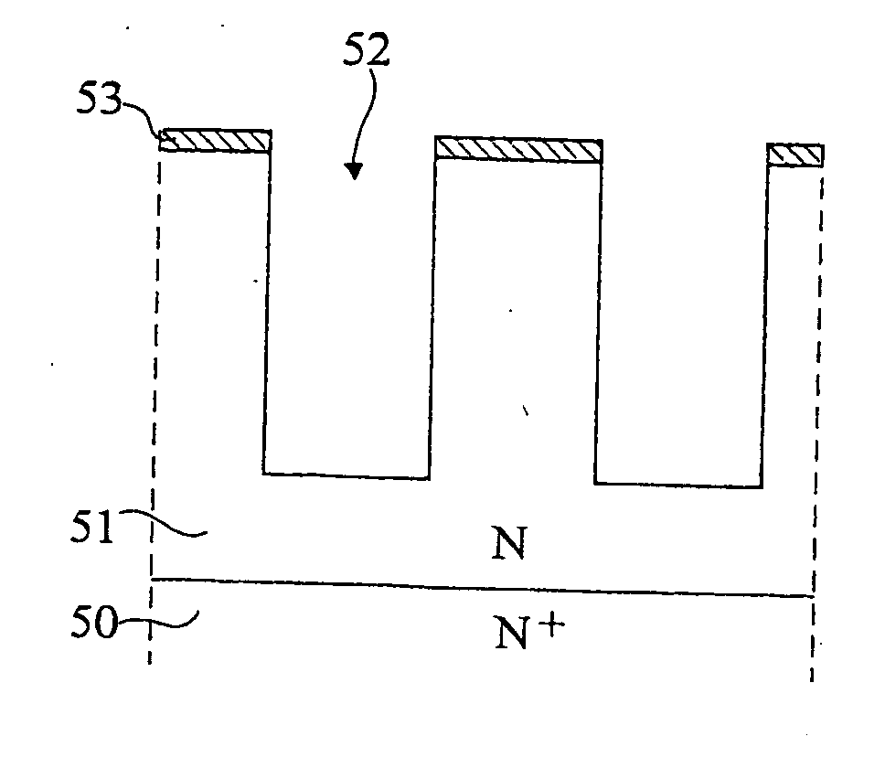
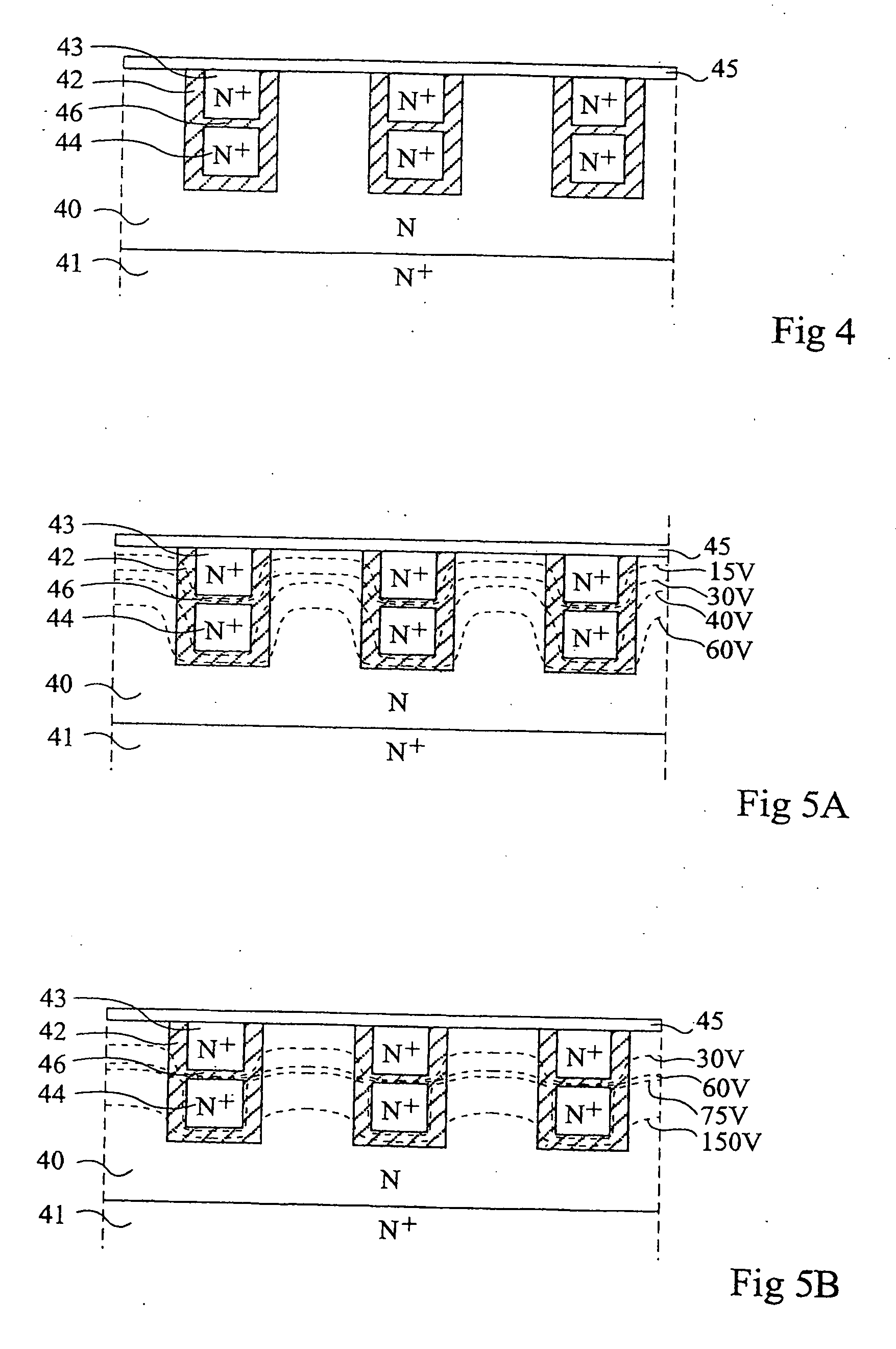
[0040]FIG. 4 is a partial simplified cross-section view of an embodiment of a Schottky diode according to the present invention. The cathode of the diode is an upper portion (N) 40 of a semiconductor substrate, for example made of single-crystal silicon. A lower portion (N+) 41 of the substrate forms a contact area of the cathode. Cathode 40 is more lightly doped than portion 41.

[0041] In cathode 40 are formed trenches coated with an insulator 42 and filled with a conductor divided in two conductive elements, a high element 43 and a low element 44 separated by an insulating layer 46. It will be said hereafter that insulated conductor elements 43-44 form a multiple-layer. The upper surface of high element 43 is coplanar with the upper surface of peripheral cathode 40 and is ...


PUM


Abstract

A vertical unipolar component formed in a semiconductor substrate. An upper portion of the substrate includes insulated trenches filled with a vertical multiple-layer of at least two conductive elements separated by an insulating layer, the multiple-layer depth being at most equal to the thickness of the upper portion.

Description

RELATED APPLICATIONS [0001] This application is a division of prior application Ser. No. 10 / 767,568, filed on Jan. 29, 2004, entitled VERTICAL UNIPOLAR COMPONENT which application is incorporated herein by reference in its entirety.BACKGROUND OF THE INVENTION [0002] 1. Field of the Invention [0003] The present invention relates to the manufacturing of vertical unipolar components in monolithic form. The following description more specifically aims, as an example only, at the case of components of Schottky diode type made in vertical form in silicon substrates. [0004] 2. Discussion of the Related Art [0005]FIG. 1 illustrates a conventional structure of a Schottky diode. The structure comprises a heavily-doped semiconductor substrate (N+) 1, typically made of single-crystal silicon. A cathode layer (N−) 2 more lightly doped than substrate 1 covers substrate 1. A metal layer 3 forms a Schottky contact with cathode 2 and forms the diode anode. The contour of anode 3 is defined by an ins...

Claims


Application Information

Patent Timeline
Patent Type & Authority Applications(United States)
IPC IPC(8): H01L21/28H01L21/44H01L29/06H01L29/40H01L29/872
CPCH01L29/404H01L29/407H01L29/7813H01L29/872H01L29/8725
Inventor LANOIS, FREDERIC
Owner STMICROELECTRONICS SRL
Features
  • R&D
  • Intellectual Property
  • Life Sciences
  • Materials
  • Tech Scout
  • Unparalleled Data Quality
  • Higher Quality Content
  • 60% Fewer Hallucinations
Learn More