CMOS image sensor and manufacturing method thereof

Inactive Publication Date: 2006-12-28
DONGBU ELECTRONICS CO LTD
View PDF24 Cites 25 Cited by
  • Summary
  • Abstract
  • Description
  • Claims
  • Application Information

AI Technical Summary

Benefits of technology

[0038] The present invention provides a CMOS image sensor with improved performance t

Problems solved by technology

The processing conditions of forming patterns may be very unstable, so the efficiency of concentrating light can be deteriorated.
However, the CMOS image sensor and the manufacturing method thereof as described above have some drawbacks as described below.
The range of viscosity that influences a thickness of the photoresist layer is strictly limited.
Accordingly, it is difficult to realize various thicknesses that are necessary in processing.
If various photoresists are used for acquiring the necessary thickness, the process is complicated.
Particularly, if a blue pho

Method used


Image

  • CMOS image sensor and manufacturing method thereof
  • CMOS image sensor and manufacturing method thereof
  • CMOS image sensor and manufacturing method thereof

Examples


Example

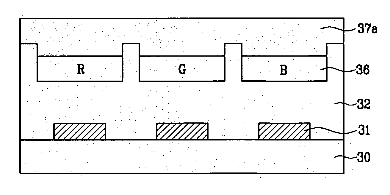
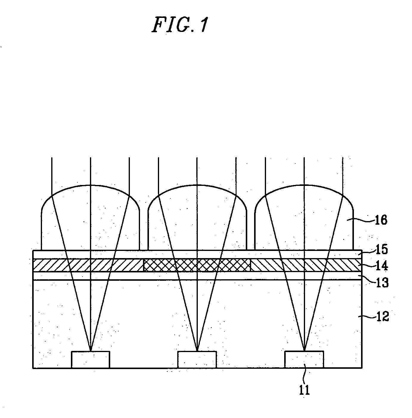
[0052] As compared to the first embodiment, the CMOS image sensor consistent with the second embodiment of the present invention includes, instead of the interlayer insulation layer 32 as shown in FIG. 3A, a passivation layer 32a for protecting photodiode regions 31 and an optical shielding layer 32b formed on the passivation layer 32a. The optical shielding layer 32b can prevent light from being incident on regions other than the photodiodes 31. As a result, a color noise is reduced. The optical shielding layer 32b may comprise silicon nitride or SiON.

[0053]FIG. 4A to FIG. 4G are cross-sectional views showing principal stages of manufacturing a CMOS image sensor consistent with the present invention, and FIG. 5 is a plan view of lattices surrounding micro-lenses in forming the CMOS image sensor.

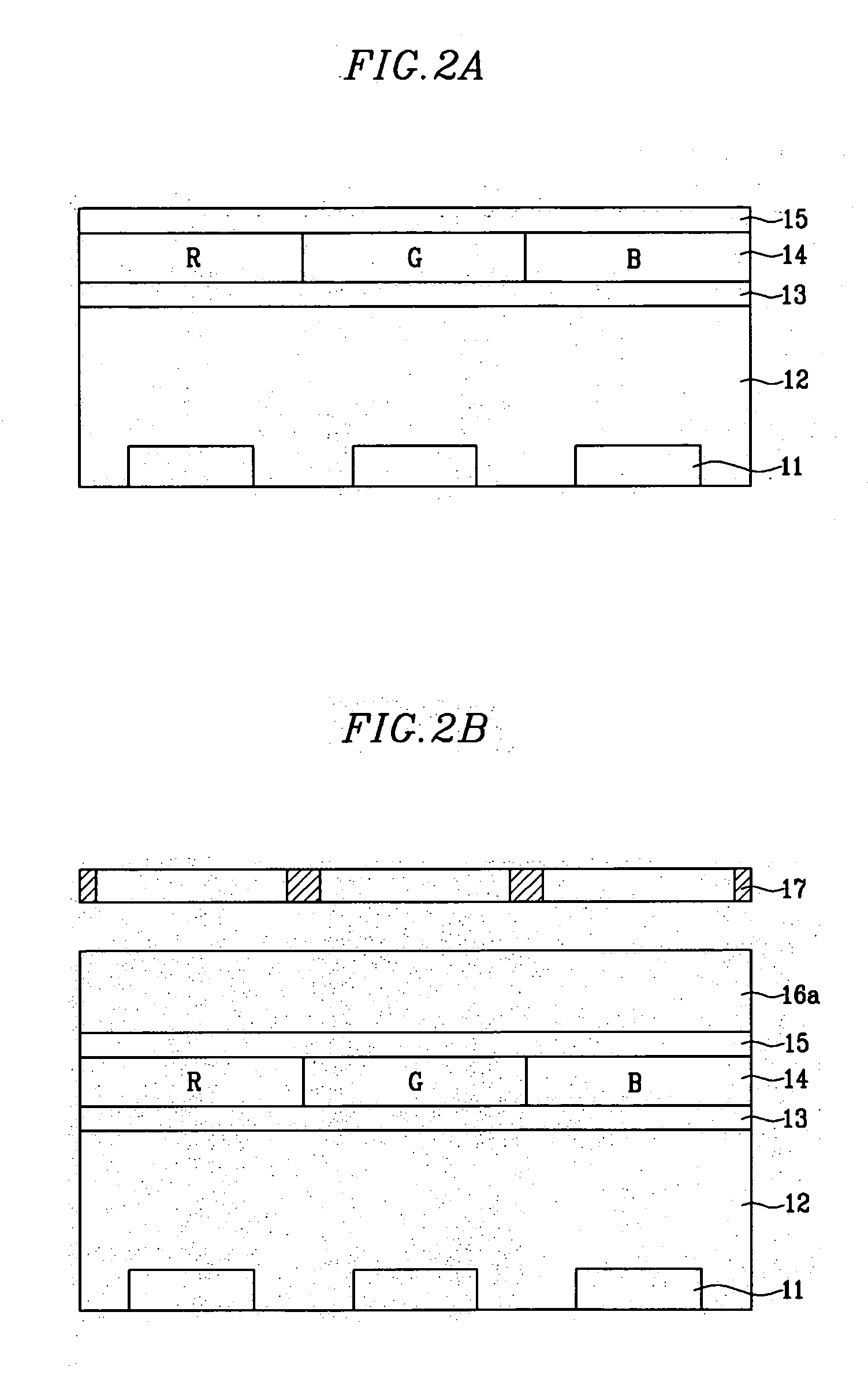
[0054] Referring to FIG. 4A, an interlayer insulation layer 32 is formed on a semiconductor substrate 30 wherein a plurality of light detecting devices such as photodiodes 31 are formed. T...

Example

[0055] Alternatively, referring to FIG. 3B and consistent with the second embodiment of the present invention, the interlayer insulation layer 32 may be formed by first forming a passivation layer 32a for protecting the photodiode regions 31 and then forming an optical shielding layer 32b on the passivation layer 32a. The optical shielding layer 32b may comprise silicon nitride or SiON.

[0056] As shown in FIG. 4B, an MUV photoresist 33, i.e., a photoresist that reacts to an I-line light, i.e., light having wavelength of 365 nm, is coated on the interlayer insulation layer 32. Subsequently, a photo mask 34 is provided over and aligned to the MUV photoresist 33. The MUV photoresist 33 is selectively exposed by illuminating light through the photo mask 34.

[0057] As shown in FIG. 4C, the exposed portion of the MUV photoresist 33 is developed so as to form a predetermined pattern. The predetermined pattern is shown in FIG. 5 as including micro-lens regions A and a lattice B surrounding ...


PUM


Abstract

A CMOS image sensor with improved performance through improved uniformity of micro-lens size and a method for manufacturing the same are provided. The CMOS image sensor includes photodiodes formed on a semiconductor substrate for producing charges consistent with a quantity of incident light, an interlayer insulation layer formed on an entire surface of the semiconductor substrate including the photodiodes , color filter layers formed in the interlayer insulation layer for passing light of respective wavelengths, and micro-lenses formed on the color filter layers for concentrating light onto the photodiodes through the color filter layers.

Description

CROSS-REFERENCE TO RELATED APPLICATION [0001] This application claims priority of benefit to Korean Patent Application No. 10-2005-0055586 filed in the Korean Intellectual Property Office on Jun. 27, 2005, the entire contents of which are incorporated herein by reference. BACKGROUND [0002] (a) Technical Field [0003] The present invention relates to an image sensor, particularly a CMOS image sensor, and a manufacturing method thereof, that can improve the performance of the image sensor by improving a uniformity of micro-lens size. [0004] (b) Description of the Related Art [0005] An image sensor is a kind of semiconductor device that can convert optical images into an electrical signal. Generally, image sensors can be divided into charge coupled device (CCD) image sensors and complementary metal oxide semiconductor (CMOS) image sensors. [0006] A CMOS image sensor is composed of a photodiode for sensing light and a CMOS logic circuit for converting the sensed light into electrical dat...

Claims


Application Information

Patent Timeline
IPC IPC(8): H01L21/00
CPCH01L27/14621H01L27/14623H01L31/0232H01L27/14685H01L31/02162H01L27/14627H01L31/02327H01L27/146
Inventor KIM, SHANG-WON
Owner DONGBU ELECTRONICS CO LTD
Why Eureka
Try Eureka