Conventionally printable non-volatile passive memory element and method of making thereof

Inactive Publication Date: 2007-03-15
NITID ACQUISITIONS LIMITED LIABILITY
View PDF23 Cites 16 Cited by
  • Summary
  • Abstract
  • Description
  • Claims
  • Application Information

AI Technical Summary

Benefits of technology

[0019] It has been surprisingly found that an element comprising a first patterned electrode system, a second patterned electrode system, an insulating system between the first patterned electrode system and the second patterned electrode system and at least one conductive or semiconducting bridge between the first patterned electrode system and the second patterned electrode system, wherein in the absence of the at least one conductive or semiconducting bridge there is no direct electrical contact between the first and the second electrode systems is printable by conventional printing processes.
[0020] Aspects of the present invention are realized by a non-volatile passive memory element comprising on a single surface a first electrode system and a second electrode system together with an insulating system, unless the insulating system is the surface, wherein the first electrode system is insulated from the second electrode system, the first and the second electrode systems are pattern systems and at least one conductive or semiconducting bridge is present between the first and second electrode systems, and wherein the non-volatile passive memory device is exclusive of metallic silicon and the systems and the conductive or semiconducting bridges are printable using conventional printing processes with the optional exception of the insulating system if the insulating system is the surface.
[0021] Aspects of the present invention are also realized by a non-volatile passive memory device comprising a support and on at least one side of the support a non-volatile passive memory element, the non-volatile passive memory element comprising on a single surface of the support a first electrode system and a second electrode system together with an insulating system, unless the insulating system is the surface, wherein the first electrode system is insulated from the second electrode system, the first and the second electrode systems are pattern systems and at least one conductive or semiconducting bridge is present between the first and second electrode systems, and wherein the non-volatile passive memory device is exclusive of metallic silicon and the systems and the conductive or semiconducting bridges are printable using conventional printing processes with the optional exception of the insulating system if the insulating system is the surface.
[0022] Aspects of the present invention have also been realized by a process for providing the above-mentioned

Problems solved by technology

Conventional silicon-based semiconductor memories have the disadvantage of requiring expensive and complex processing, the high process temperatures and the non-flexibility making them unsuitable for use on packaging substrates.
Moreover, silicon-based semiconductor memories pose considerable environmental issues upon disposal.
However, this does not prevent the existence of alternative current paths.
However, the production processes for the resistor memory cells disclosed in U.S. Pat. Nos. 6,107,666, US 6,542,397 and US 6,649,499 all rely on evaporation and etching methods to apply the metal or silicon structures, requiring high temperatures in the range of 300° C. to 400° C., which results in melting or severe degradation of polymer-based or paper-based substrates, hence making it unsuitable for packaging.
Therefore such metal or silicon structures neither lend themselves to incorporation into tag, label and package printing process or into the packaging process nor do they lend themselves to environmentally friendly disposal.
To prevent alternative current paths it is necessary to include additional layers between the word lines and bit lines in each memory cell to form diodes, hereby making the manufacturing process more complicated.
However, these memories are volatile, and the information is lost if no power is applied.

Method used


Image

  • Conventionally printable non-volatile passive memory element and method of making thereof
  • Conventionally printable non-volatile passive memory element and method of making thereof
  • Conventionally printable non-volatile passive memory element and method of making thereof

Examples


invention example 1

Fully Ink-jet Printed Non-volatile Passive Memory Device

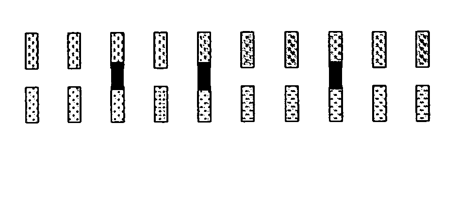
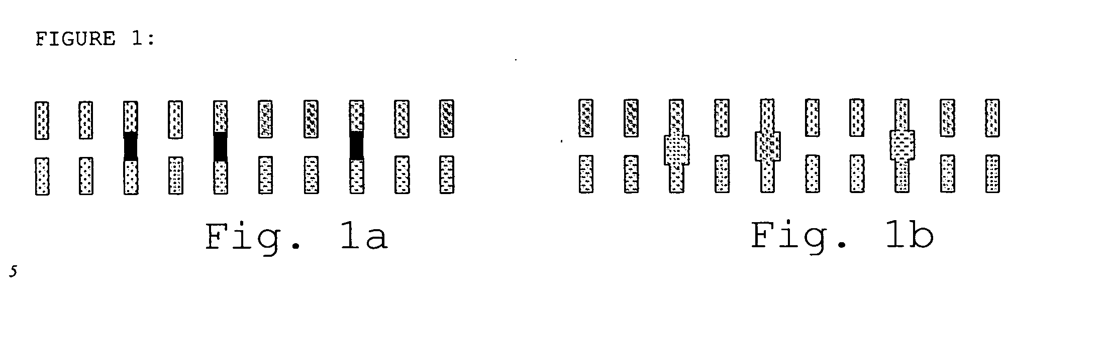
[0127] The first and second electrode systems were ink-jet printed with appropriate electrical contacts for reading out the stored information in contact on the subbed side of SUPPORT 01 from a Universal Printhead (from AGFA-GEVAERT) using the ink-jet ink, the surface of the subbing layer providing the insulating system. A non-volatile passive memory device precursor is thereby provided. Conductive bridges were then provided by ink-jet printing the ink-jet ink from a Universal Printhead (from AGFA-GEVAERT) between predesignated points of the first and the second electrode systems to produce a non-volatile passive memory device.

invention example 2

Flexographically / Ink Jet Printed Non-volatile Passive Memory Device

[0128] The first and second electrode systems were printed with appropriate electrical contacts for reading out the stored information in contact by flexographic printing using a Rotary Koater Pilot Press (from R.K. Print Coat Instruments, Ltd.) on SUPPORT 02 using the flexographic ink and then drying in an oven at 109° C. in a roll to roll process, the PET surface providing the insulating system. A non-volatile passive memory device precursor is thereby provided. conductive bridges were then provided by ink-jet printing the ink-jet jet ink from a Universal Printhead (from AGFA-GEVAERT) between predesignated points of the first and the second electrode systems to provide a non-volatile passive memory device.

invention example 3

Flexographically / Ink Jet Printed Non-volatile Passive Memory Device

[0129] The first and second electrode systems were printed with the appropriate electrical contacts required for reading out the stored information in contact by flexographic printing using a Rotary Koater Pilot Press (from R.K. Print Coat Instruments, Ltd.) on SUPPORT 03 using the flexographic ink and then drying in an oven at 109° C. in a roll to roll process, the surface of the subbing layer providing the insulating system. A non-volatile passive memory device precursor is thereby provided. Conductive bridges were then provided by ink-jet printing the ink-jet ink from a Universal Printhead (from AGFA-GEVAERT) between predesignated points of the first and the second electrode systems to provide a non-volatile passive memory device.


PUM


Abstract

A non-volatile passive memory element comprising on a single surface a first electrode system and a second electrode system together with an insulating system, unless the insulating system is the surface, wherein the first electrode system is insulated from the second electrode system, the first and the second electrode systems are pattern systems and at least one conductive or semiconducting bridge is present between the first and second electrode systems, and wherein the non-volatile passive memory device is exclusive of metallic silicon and the systems and the conductive or semiconducting bridges are printable using conventional printing processes with the optional exception of the insulating system if the insulating system is the surface. A non-volatile passive memory device comprising a support and on at least one side of the support the above-mentioned non-volatile passive memory element. A process for providing the above-mentioned non-volatile passive memory device, comprising the realization on a single surface of the support of the steps of: providing a first electrode system pattern, optionally providing an insulating pattern, providing a second electrode system pattern, and providing at least one conductive or semiconducting bridge between the first electrode system pattern and the second electrode system pattern at predesignated points, wherein at least one of the steps is realized with a conventional printing process and two of said steps are optionally performed simultaneously.

Description

CROSS-REFERENCE TO RELATED PATENT APPLICATIONS [0001] This application is a continuation in part of U.S. application Ser. No. 11 / 260,832 filed Oct. 27, 2005, which claims the benefit of U.S. Provisional Application No. 60 / 630,185 filed Nov. 22, 2004, which is incorporated by reference therein and the benefit of European Application No. 04105412.3 filed Oct. 29, 2004, which is also incorporated therein by reference.FIELD OF THE INVENTION [0002] The present invention concerns a conventionally printable non-volatile passive memory element, a conventionally printable non-volatile memory device precursor, a conventionally printable non-volatile memory device and methods of making a conventionally printable non-volatile memory device. BACKGROUND OF THE INVENTION [0003] There is currently an increasing demand for disposable, inexpensive, flexible, passive memory device-containing tags and labels in which information is stored, for example as anti-counterfeiting tags in packaging. Productio...

Claims


Application Information

Patent Timeline
IPC IPC(8): H01L29/788
CPCB82Y10/00G11C11/5664G11C11/5692G11C2213/80G11C13/0014G11C13/0016G11C17/00G11C13/00
Inventor LEENDERS, LUCWERTS, MICHEL
Owner NITID ACQUISITIONS LIMITED LIABILITY
Why Eureka
Try Eureka