Unlock instant, AI-driven research and patent intelligence for your innovation.

Semiconductor memory device and memory module

a memory module and semiconductor technology, applied in the field of semiconductor memory devices and memory modules, can solve the problems of preventing the accurate determination of logic levels, affecting the accuracy of logic determination, and difficulty in taking measures such as decoupling and the like on the circuit board of the memory module, so as to achieve sufficient attenuation, eliminate unnecessary high-frequency components, and prevent malfunction

Active Publication Date: 2007-04-19
LONGITUDE LICENSING LTD
View PDF13 Cites 9 Cited by
  • Summary
  • Abstract
  • Description
  • Claims
  • Application Information

AI Technical Summary

Benefits of technology

[0009] It is an object of the invention to provide a semiconductor memory device and memory module capable of reliably eliminating noise components of a reference signal caused by an operating clock and the like when a reference voltage is supplied to the semiconductor memory device by an external reference signal, and of effectively preventing malfunction due to the effect of the noise.
[0010] An aspect of the present invention is a semiconductor memory device which determines a logic level of a signal based on a predetermined reference voltage comprising: an input terminal to which a reference signal having said reference voltage is input; a low-pass filter connected to said input terminal for passing a component of said reference voltage of said reference signal and eliminating undesired high frequency components; and one or more input first-stage circuits to each of which an output of said low-pass filter and a signal having said logic level to be determined are connected, wherein said low-pass filter has a predetermined attenuation amount at least at a frequency of an operating clock.
[0011] According to an aspect of the semiconductor memory device of the invention, when a reference signal with which noise is mixed is input from outside the semiconductor memory device, high-frequency noise components are eliminated by the low-pass filter placed immediately near the input terminal. In this case, the reference voltage which is a DC component is maintained, while it is possible to reliably attenuate the noise near an operating clock frequency which particularly has a significant effect. Then, in the input first-stage circuits, the logic level of a signal can be determined based on the reference voltage without noise, and it is thus possible to effectively prevent malfunction due to noise.
[0018] As described above, according to the present invention, the low-pass filter is inserted between the input terminal for the reference signal having the reference voltage and the input first-stage circuits for various signals, so that unnecessary high-frequency components are eliminated. Therefore, it is possible to reliably eliminate high-frequency noise components mixed with the reference signal due to the operating clock and the like. By this means, it is possible to determine the logic level of a signal based on the high-accurate reference signal without noise, and malfunction can be prevented effectively in the input first-stage circuits.
[0019] In the present invention, when employing a passive low-pass filter, it is possible to obtain a sufficient amount of attenuation using a simple configuration. Meanwhile, when employing an active low-pass filter, as well as blocking noise from outside to the inside of the semiconductor memory device, it is possible to block noise from the semiconductor memory device to outside. Further, when applying the present invention to a memory module, even in a configuration in which a plurality of DRAM chips shares the reference voltage, it is possible to suppress mutual influences of noise between the chips.

Problems solved by technology

In this case, since a frequency band of the noise is of order of 100 MHz, it is difficult to take measures such as decoupling and the like on the circuit board of the memory module.
In particular, if the noise is mixed with the VREF signal and transmitted through the common wiring, it becomes a problem that malfunction of the DRAM chip occurs.
That is, since the VREF signal used to determine the logic level of a signal has a low tolerance for noise, it is feared that a slight variation in the level prevents the accurate determination of the logic level.
However, such a filter is provided mainly to avoid EMC problem of the semiconductor chip, and is not effective as measures against the malfunction due to the VREF signal requiring high accuracy.

Method used


Image

  • Semiconductor memory device and memory module
  • Semiconductor memory device and memory module
  • Semiconductor memory device and memory module

Examples


first embodiment

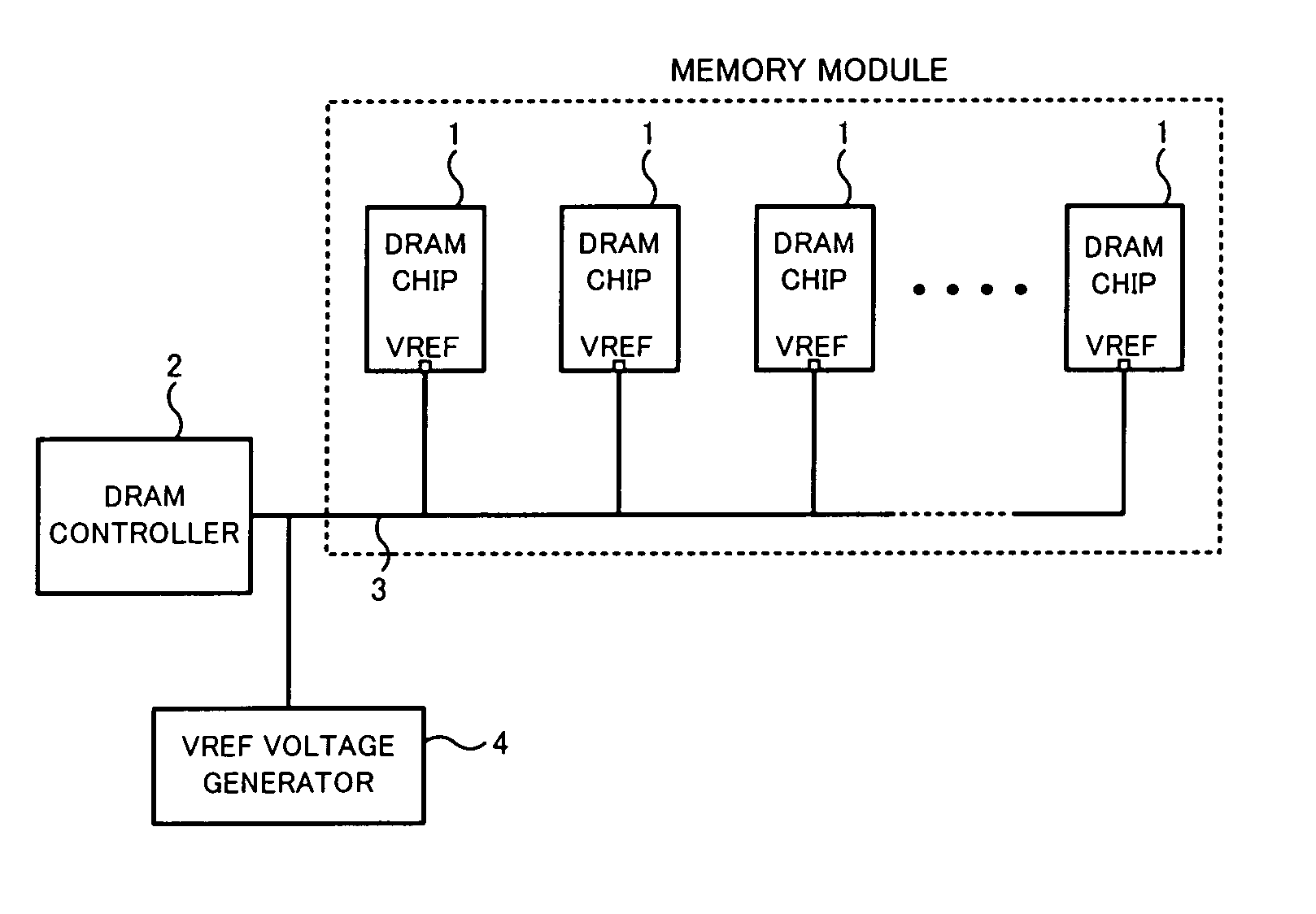
[0030] In the first embodiment, the invention is applied to a memory module in which a plurality of semiconductor memory devices is integrally connected. FIG. 1 is a diagram showing an entire configuration including the memory module of the first embodiment. FIG. 2 is a diagram showing a principal configuration of the semiconductor memory device (DRAM chip 1) included in the memory module of the first embodiment. As shown in FIG. 1, the memory module of the first embodiment has a configuration in which a plurality of DRAM chips 1 is mounted as semiconductor memory devices and a DRAM controller 2 controls operation of each of the DRAM chips 1. Generally, the entire memory module as shown in FIG. 1 is mounted on a single circuit board.

[0031] The DRAM controller 2 supplies a number of control signals (not shown) to respective DRAM chips 1. A VREF voltage generator 4 generates a VREF signal (reference signal) used as a reference voltage to supply to each DRAM chip 1 and the DRAM contro...

second embodiment

[0049] In the second embodiment, the present invention is applied to a DRAM chip in which the configuration of the low-pass filter 10 of the above-mentioned first embodiment is modified. FIG. 6 is a diagram showing a principal configuration of the DRAM chip 1 as a semiconductor memory device of the second embodiment. The entire configuration including the memory module of the second embodiment is the same as in FIG. 1.

[0050] As shown in FIG. 6, the DRAM chip 1 of the second embodiment has an active low-pass filter 11 inserted between the VREF terminal and input first-stage circuits A0 to An-1. The active low-pass filter 11 has a circuit configuration including active elements such as MOS transistors, and as in the low-pass filter 10 of the first embodiment, has the function of passing a DC component of the VREF signal and eliminating unnecessary high-frequency components. In FIG. 6, the VREF signal, the DQ0 to DQn-1 terminals and the input first-stage circuits A0 to An-1 have the s...


PUM


Abstract

A semiconductor memory device of the present invention determines a logic level of a signal based on a predetermined reference voltage. And the memory device has an input terminal to which a reference signal having the reference voltage is input, a low-pass filter connected to the input terminal for passing a component of the reference voltage of the reference signal and eliminating undesired high frequency components, and one or more input first-stage circuits to each of which an output of the low-pass filter and a signal having the logic level to be determined are connected. In the memory device, the low-pass filter has predetermined attenuation at least at a frequency of an operating clock.

Description

BACKGROUND OF THE INVENTION [0001] 1. Field of the Invention [0002] This invention relates to a technical field of a semiconductor memory device having a configuration in which a logic level of a signal is determined based on a reference signal input from outside and a memory module in which a plurality of the above-mentioned semiconductor memory devices are connected to form an integrated memory. [0003] 2. Description of the Related Art [0004] Memory modules having a plurality of semiconductor memory devices connected integrally have been conventionally used widely to construct a large capacity memory system. For example, a memory module having a configuration in which a plurality of DRAM chips is mounted on a circuit board and required signals can be transmitted through common wiring between a memory controller and the DRAM chips is employed. [0005] Generally, in the DRAM chip, a signal having a reference voltage (herein after referred to as a VREF signal) is necessary to determin...

Claims


Application Information

Patent Timeline
IPC IPC(8): H03B1/00
CPCG11C5/147G11C11/4074H03F3/45183
Inventor IDEI, YOJIHATANO, SUSUMUNISHIO, YOJIFUNABA, SEIJIUEMATSU, YUTAKA
Owner LONGITUDE LICENSING LTD