Lvds output driver
- Summary
- Abstract
- Description
- Claims
- Application Information
AI Technical Summary
Benefits of technology
Problems solved by technology
Method used
Image

Examples
Embodiment Construction
[0016]The following description is of the best-contemplated mode of carrying out the invention. This description is made for the purpose of illustrating the general principles of the invention and should not be taken in a limiting sense. The scope of the invention is best determined by reference to the appended claims.
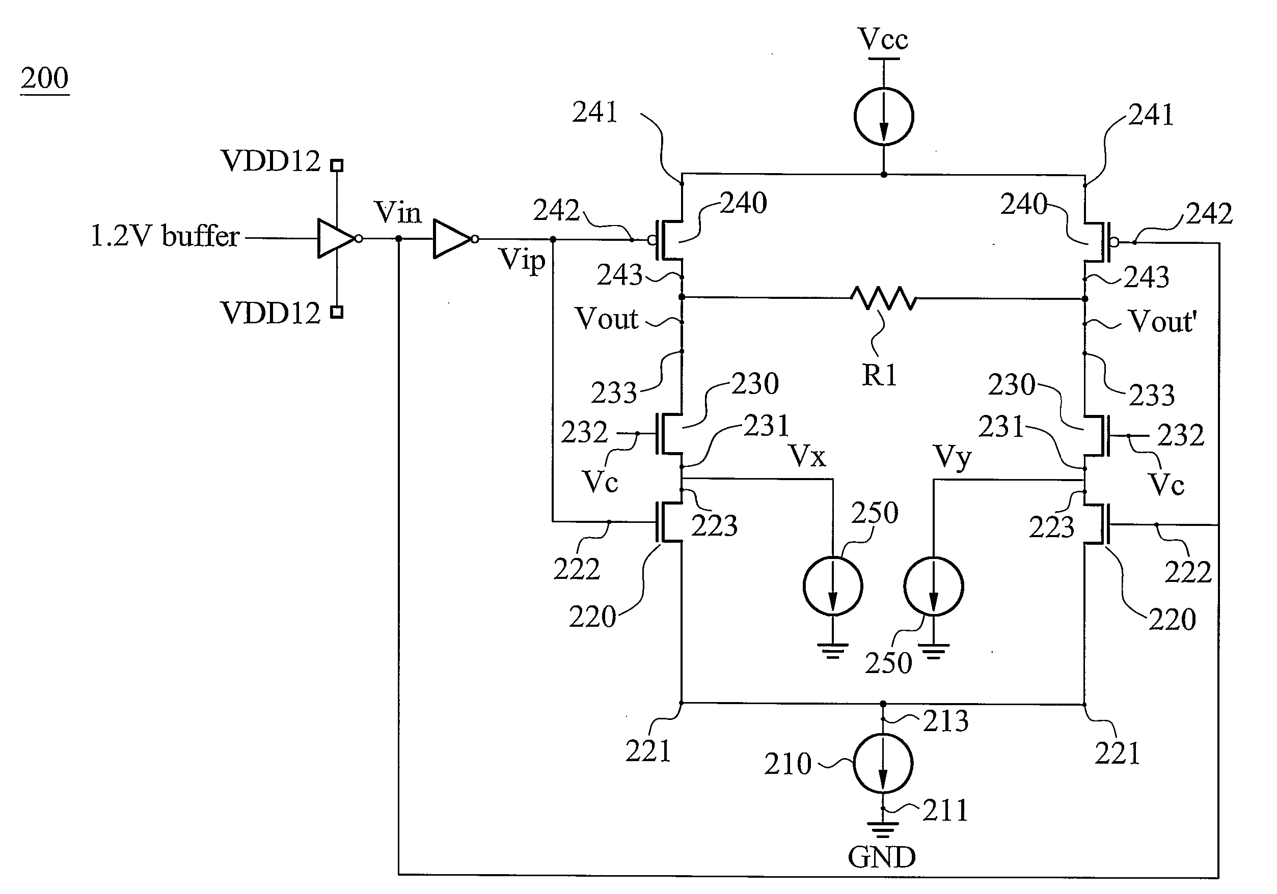
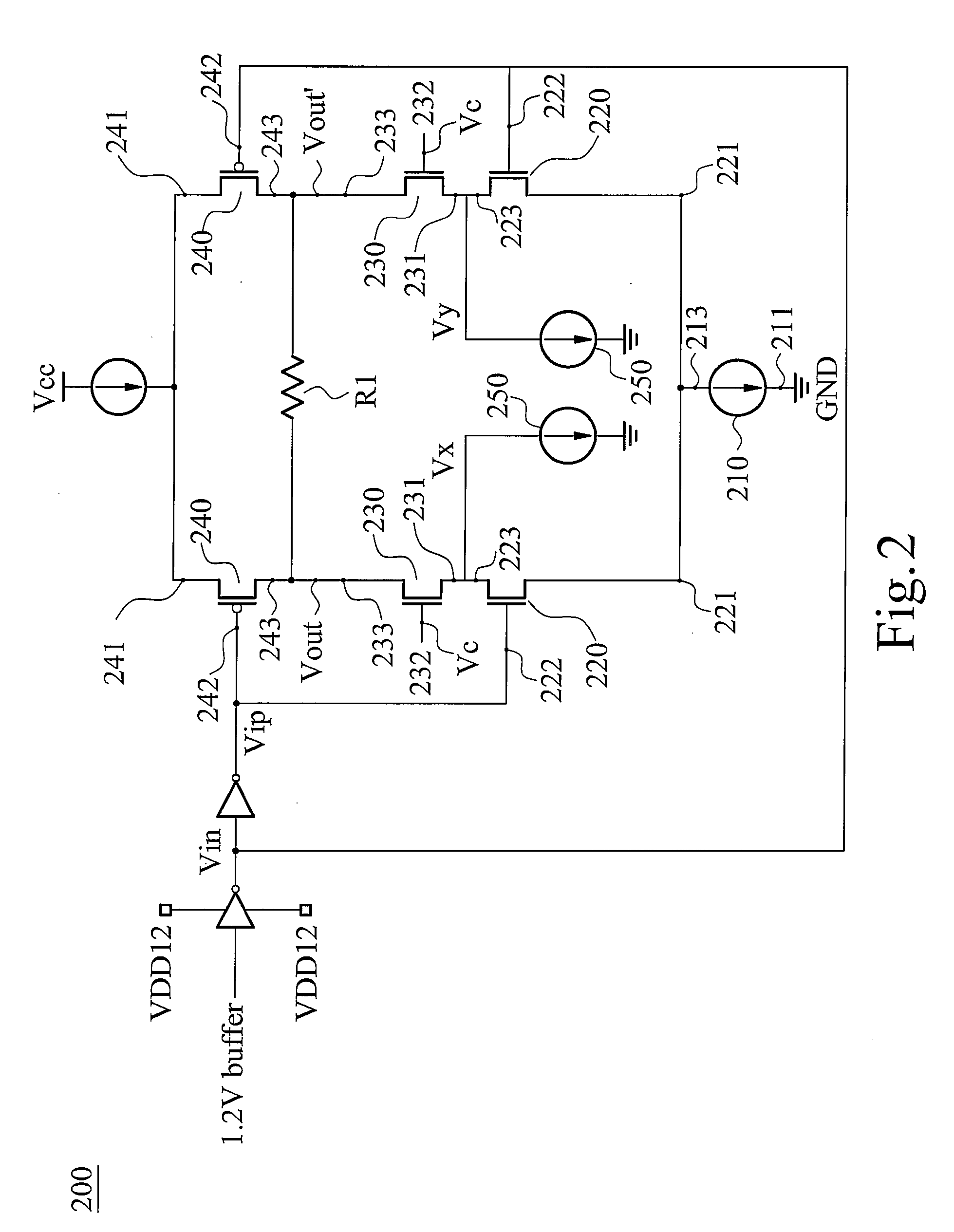
[0017]FIG. 2 is a circuit diagram of an output driver 200 according to an embodiment of the invention. A pair of differential outputs Vout and Vout′ of the output driver 200 is coupled to a first supply voltage via a pair of load devices 240. More specifically, the first supply voltage is a power voltage Vcc. The voltage value of Vcc depends on the requirement of the channel connected to the pair of differential outputs Vout and Vout′. Typically, the power voltage Vcc could be approximately 3 Volt in an LVDS output driver. In the embodiment, the load devices are high voltage PMOS transistors 240, which are namely IO devices utilized in IC chips. Each of the PMOS transi...
PUM
 Abstract
Description
Claims
Application Information
 - R&D Engineer
- R&D Manager
- IP Professional
- Industry Leading Data Capabilities
- Powerful AI technology
- Patent DNA Extraction
Browse by: Latest US Patents, China's latest patents, Technical Efficacy Thesaurus, Application Domain, Technology Topic.
© 2024 PatSnap. All rights reserved.Legal|Privacy policy|Modern Slavery Act Transparency Statement|Sitemap