Check patentability & draft patents in minutes with Patsnap Eureka AI!

Semiconductor light-emitting device

a technology semiconductor, which is applied in the direction of semiconductor light-emitting device, basic electric element, electrical apparatus, etc., can solve the problems of adverse effect on the performance of the semiconductor light-emitting device and the light extraction efficiency of the led decrease, so as to improve the light extraction efficiency and reliability

Inactive Publication Date: 2009-10-01
LITE ON ELECTRONICS (GUANGZHOU) LTD +1
View PDF3 Cites 25 Cited by
  • Summary
  • Abstract
  • Description
  • Claims
  • Application Information

AI Technical Summary

Benefits of technology

[0010]Therefore, an object of the present invention is to provide a semiconductor light-emitting device with improved light extraction efficiency and reliability.

Problems solved by technology

However, the aforesaid reflector can also focus the light emitted from the fluorescent layer on the LED chip, thereby resulting in absorption of the light reflected from the reflector by the LED chip, and in a decrease in the light extraction efficiency of the LED.
Moreover, since the surface of the aforesaid reflector is relatively smooth, an adhesion force between the reflector and an encapsulant that fills a space between the reflector and the LED chip is relatively weak, and moisture is likely to penetrate into the semiconductor light-emitting device, which has an adverse effect on performance of the semiconductor light-emitting device.

Method used


Image

  • Semiconductor light-emitting device
  • Semiconductor light-emitting device
  • Semiconductor light-emitting device

Examples


Embodiment Construction

[0017]According to geometrical optics, when light is emitted from a light source toward a medium, part of it would be reflected by the medium, part of it would pass through the medium, and part of it would be absorbed by the medium. The relationship between light and the medium satisfies the following equation:

Reflectivity+Transparency+Absorptivity=1

[0018]The reflectivity is composed of a diffuse reflectivity and a specular reflectivity. The diffuse surface defined hereinafter in the present invention is a surface that has a diffuse reflectivity larger than the specular reflectivity when reflection of light occurs on the diffuse surface. In other words, as long as a surface has a diffuse reflectivity larger than the specular reflectivity, the surface can be regarded as a diffuse surface.

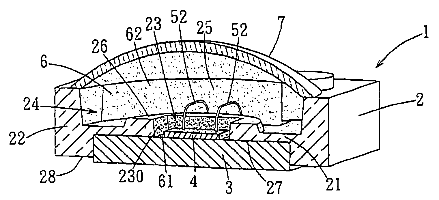
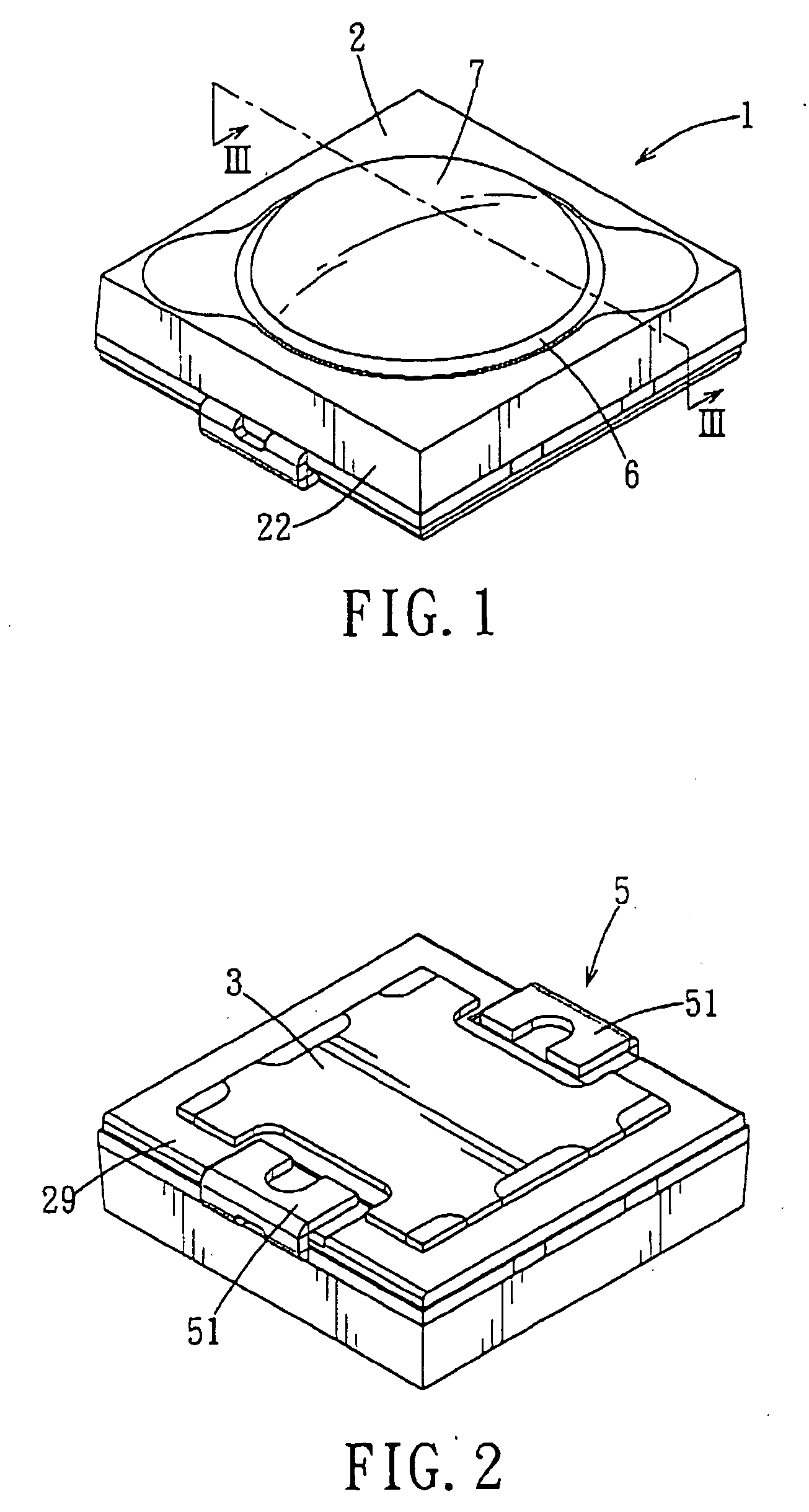
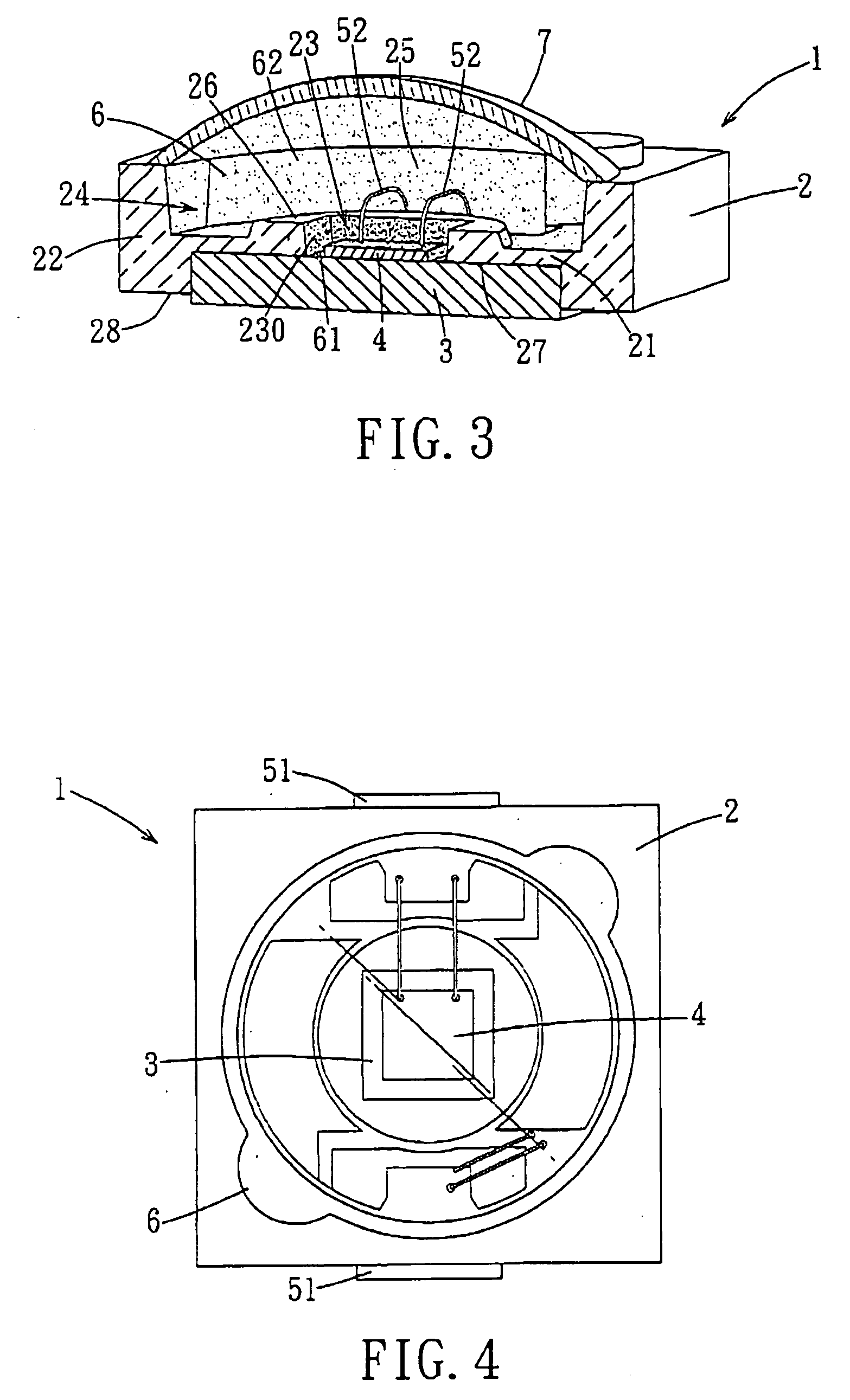
[0019]Referring to FIGS. 1 to 4, the semiconductor light-emitting device 1 of the preferred embodiment of the present invention is shown to include a hollow body 2, a heat-dissipating body 3, a light...


PUM


Abstract

A semiconductor light-emitting device includes: a hollow body including a bottom wall and a surrounding wall cooperating with the bottom wall to define an encapsulant-receiving recess, the bottom wall being formed with a through-hole, the surrounding wall having a diffuse surface that surrounds the encapsulant-receiving recess; a heat-dissipating body provided on a bottom side of the bottom wall and covering the through-hole in the bottom wall; a light-emitting chip disposed in the through-hole in the bottom wall; a transparent encapsulant filling the encapsulant-receiving recess and the through-hole; and a wavelength-converting layer covering the transparent encapsulant.

Description

CROSS-REFERENCE TO RELATED APPLICATION[0001]This application claims priority of Chinese application no. 200810027087.6, filed on Mar. 25, 2008.BACKGROUND OF THE INVENTION[0002]1. Field of the Invention[0003]This invention relates to a semiconductor light-emitting device, more particularly to a semiconductor light-emitting device having a function of diffusing light so as to enhance light extraction efficiency thereof.[0004]2. Description of the Related Art[0005]A conventional semiconductor light-emitting device usually uses light emitting diode(s) (LEDs) as a light source, and a fluorescent layer which includes fluorescent powders that are excited to emit light of a predetermined color when the LED is activated.[0006]Currently, the fluorescent layer is normally applied to the semiconductor light-emitting device by a “conformal coating” method or a “remote phosphor” method. In the “conformal coating” method, the fluorescent layer containing fluorescent powders is disposed to surround...

Claims


Application Information

Patent Timeline
Patent Type & Authority Applications(United States)
IPC IPC(8): H01L33/00H01L33/48H01L33/50H01L33/64
CPCH01L33/486H01L33/507H01L33/642H01L2224/48091H01L2924/00014
Inventor CHANG CHIEN, CHIEN-LINSU, HUNG-YUANLIN, CHEN-HSIU
Owner LITE ON ELECTRONICS (GUANGZHOU) LTD
Features
  • R&D
  • Intellectual Property
  • Life Sciences
  • Materials
  • Tech Scout
  • Unparalleled Data Quality
  • Higher Quality Content
  • 60% Fewer Hallucinations
Learn More