Check patentability & draft patents in minutes with Patsnap Eureka AI!

Bias circuit and control method for bias circuit

Inactive Publication Date: 2010-08-19
FUJITSU LTD
View PDF12 Cites 3 Cited by
  • Summary
  • Abstract
  • Description
  • Claims
  • Application Information

AI Technical Summary

Benefits of technology

The present invention provides a bias circuit and control method for a bias circuit that can inhibit fluctuations of characteristics, operate at a high speed, and apply a threshold voltage to a nonlinear amplifier. The bias circuit includes a constant-current source and transistors connected in a specific configuration to achieve these technical effects. The technical effects include improved stability and accuracy of the amplifier, as well as improved production yield.

Problems solved by technology

However, although Vth+α is applied as the bias voltage, a B-class amplifier does not operate as the B-class amplifier.

Method used


Image

  • Bias circuit and control method for bias circuit
  • Bias circuit and control method for bias circuit
  • Bias circuit and control method for bias circuit

Examples


Embodiment Construction

[0037]The best mode for carrying out the invention will be described below.

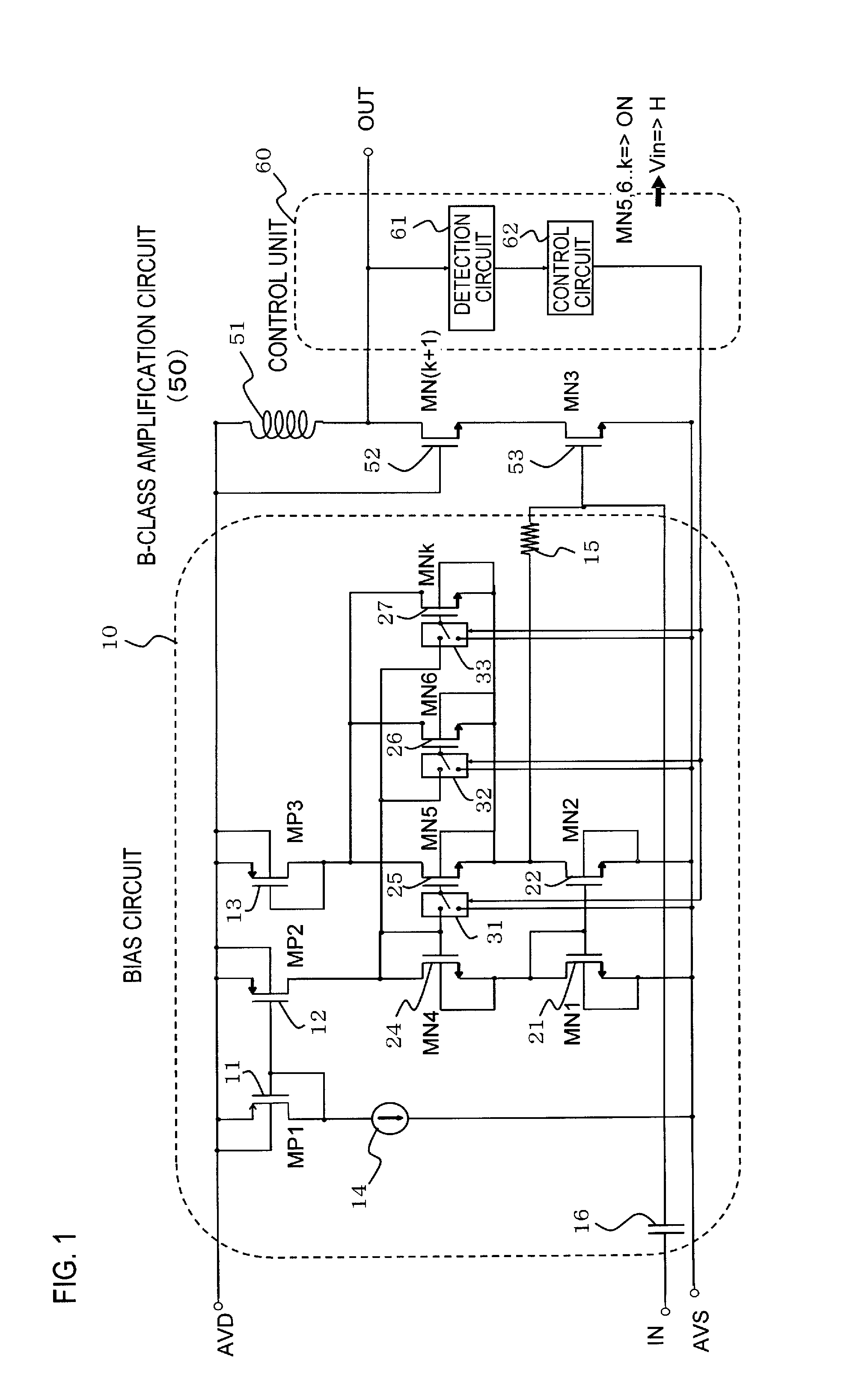
[0038]FIG. 1 illustrates configuration examples of a bias circuit 10, a B-class amplification circuit 50, and a control unit 60.

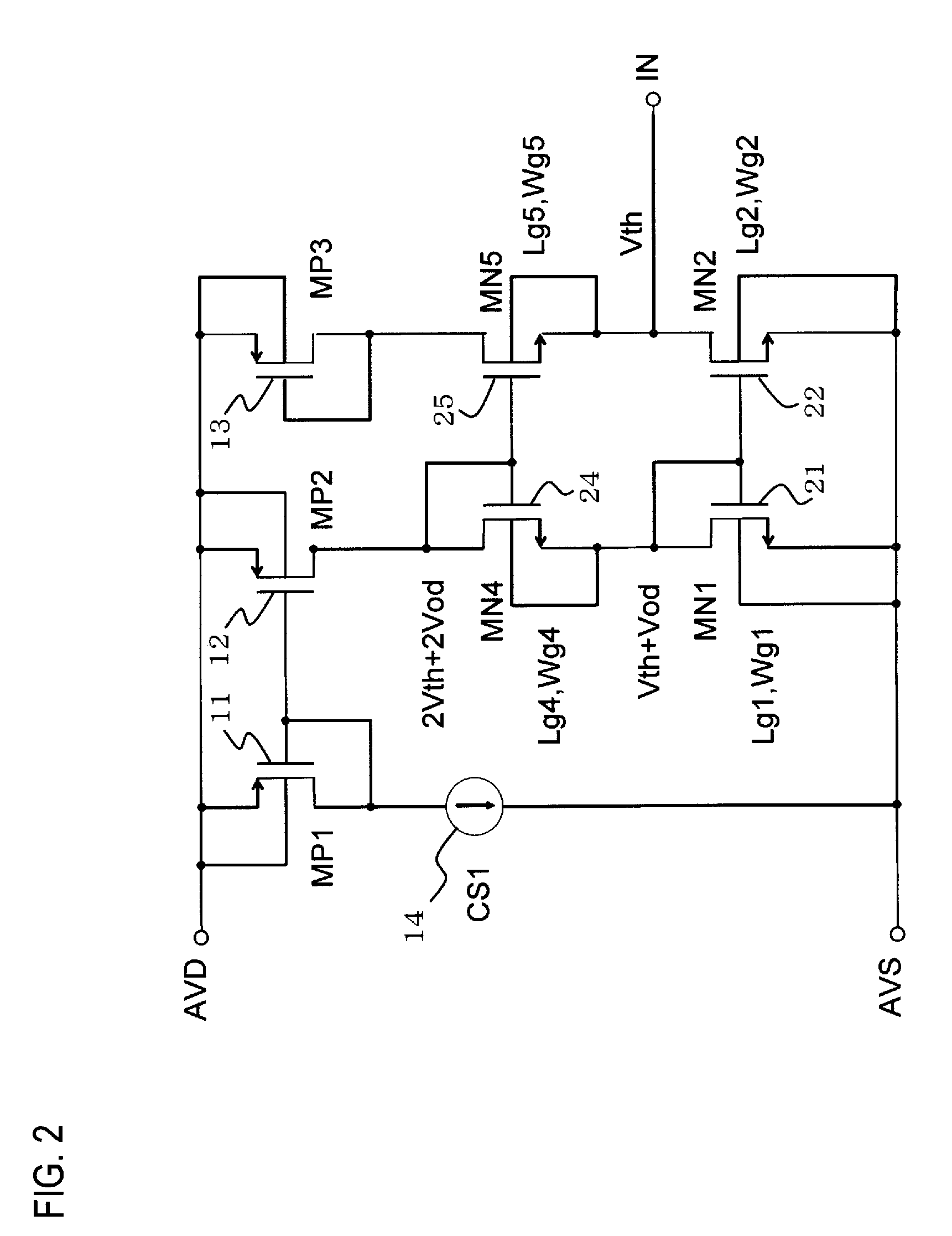
[0039]The bias circuit 10 includes a first to third p-channel transistors (referred to hereinbelow as p-type transistors) (MP1, MP2, MP3) 11, 12, 13, a constant-current source 14, a resistor 15, a capacitor 16, a first and second n-channel transistors (referred to hereinbelow as n-type transistors) (MN1, MN2) 21, 22, and a fourth to k-th n-type transistors (MN4, MN5, . . . , MNk; k is integer equal to or greater than 7) 24, 25, 26, 27. The bias circuit 10 serves to apply a bias voltage to the B-class amplification circuit 50.

[0040]The B-class amplification circuit 50 includes a coil 51, a (k+1)-th n-type transistor (MN(k+1)) 52, and a third n-type transistor (MN3) 53. The B-class amplification circuit 50 is a nonlinear amplification circuit that amplifies only one polarity of inputte...


PUM


Abstract

A bias circuit for applying a bias voltage to a nonlinear amplification circuit, including a constant-current source; and a first, second, third, and fourth transistors, wherein a current mirror circuit is configured by the first transistor and the second transistor, and the bias voltage is outputted from the drain of the second transistor, gate lengths and gate widths of the first and second transistor are the same, gate lengths of the first to fourth transistor are the same, and gate lengths and gate widths of the first, second, third, and fourth transistor are configured so that k4−0.5−k3−0.5 is approximately 1, where k3 stands for a ratio of a gate width of the third transistor to the gate width of the first transistor and k4 stands for a ratio of a gate width of the fourth transistor to the gate width of the first transistor.

Description

CROSS-REFERENCE TO RELATED APPLICATIONS[0001]This application is a continuation of International Application No. PCT / JP2007 / 1247, filed on Nov. 16, 2007, now pending, herein incorporated by reference.TECHNICAL FIELD[0002]The present invention relates to a bias circuit and a control method for a bias circuit.BACKGROUND ART[0003]A bias circuit is connected to an amplifier and applies a constant bias voltage with respect to an input signal to the amplifier.[0004]A circuit 100 illustrated in FIG. 7 includes a constant-current source (CS1) 101, first and second transistors (MN1, MN2) 102, 104, and resistor 103. Of these components, a bias circuit is configured by the constant-current source (CS1) 101 and the first transistor (MN1) and applies a bias voltage to an amplifier configured by a coil 106 and a transistor (MN3) 105.[0005]A variety of bias circuits have heretofore been suggested (see, for example, the following Patent Document 1 to Patent Document 3).[0006]Patent Document 1: Japa...

Claims


Application Information

Patent Timeline
Patent Type & Authority Applications(United States)
IPC IPC(8): H03F3/16
CPCH03F1/223H03F1/301H03F2200/456H03F2200/18H03F2200/108
Inventor ARAI, TOMOYUKIKUDO, MASAHIRO
Owner FUJITSU LTD
Features
  • R&D
  • Intellectual Property
  • Life Sciences
  • Materials
  • Tech Scout
  • Unparalleled Data Quality
  • Higher Quality Content
  • 60% Fewer Hallucinations
Learn More