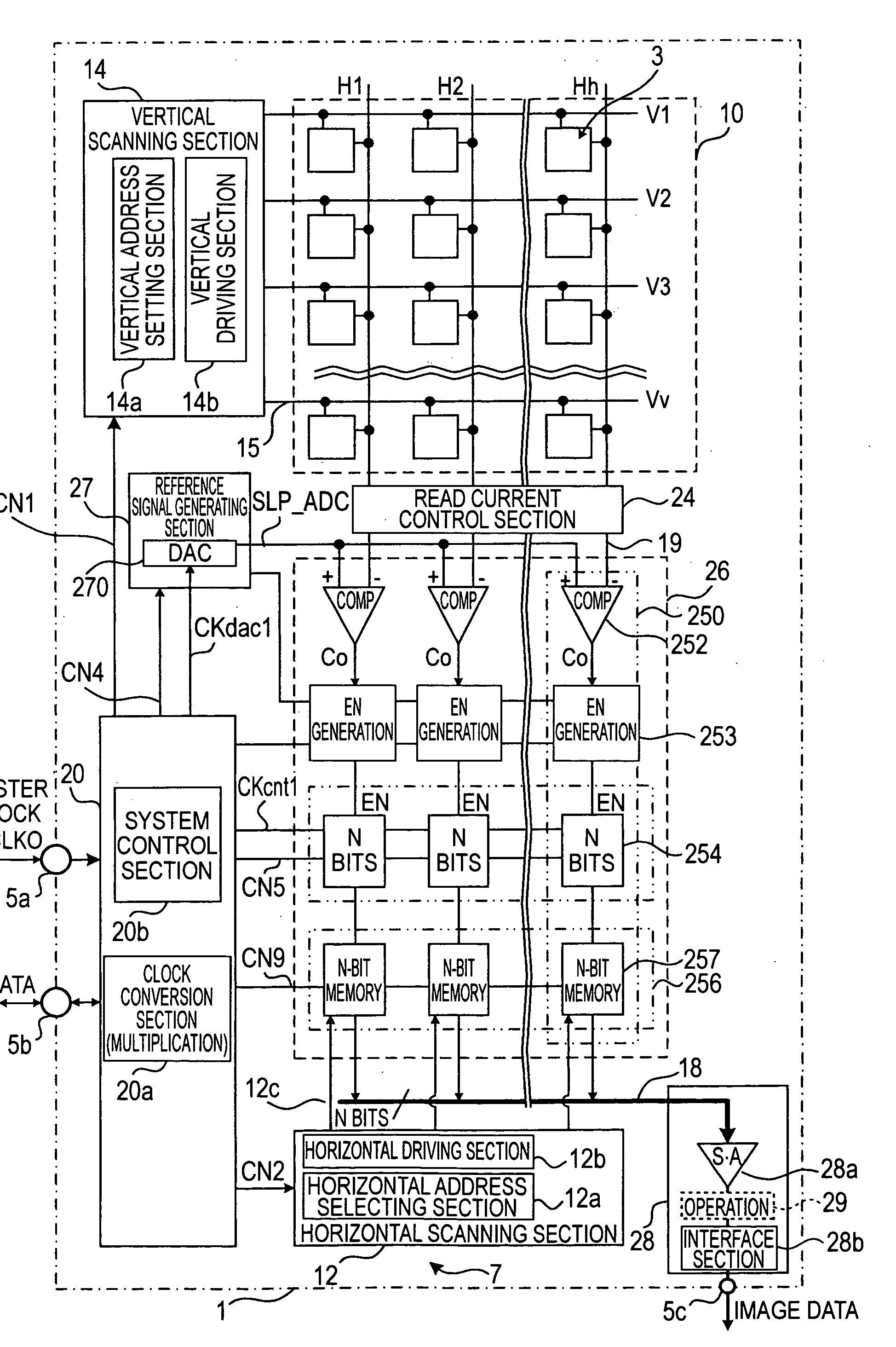
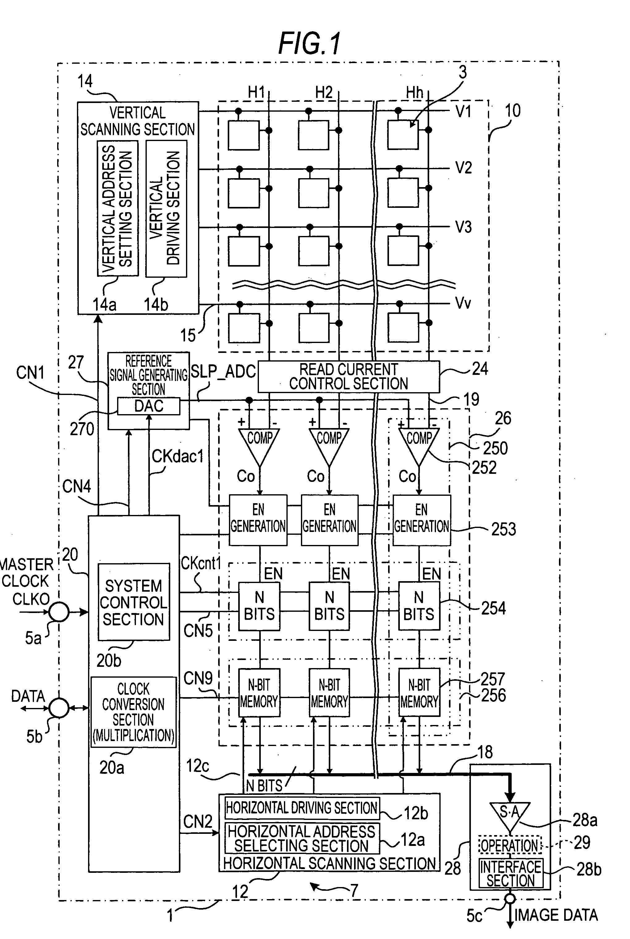
Solid state imaging device, imaging apparatus, electronic apparatus, AD converter, and AD conversion method
a technology of solid-state imaging and imaging apparatus, which is applied in the direction of television systems, pulse techniques, instruments, etc., can solve the problems of circuit size or precision, power consumption caused by counter operation, and large circuit size, so as to shorten the operating time of the counter without decreasing the bit precision, the effect of low power consumption
- Summary
- Abstract
- Description
- Claims
- Application Information
AI Technical Summary
Benefits of technology
Problems solved by technology
Method used
Image

Examples
first embodiment
[0184]FIGS. 4A to 4E are views illustrating a first embodiment. In the first embodiment, AD processing is performed twice similar to the processing shown in FIG. 3C. Here, FIG. 4A is a view showing the simple circuit configuration of a solid state imaging device 1A according to the first embodiment when AD conversion processing and CDS processing are taken into consideration. FIG. 4B is a view showing an example of the configuration of the comparing section 252 used in the solid state imaging device 1A according to the first embodiment. FIG. 4C is a view showing an example of the detailed configuration of a part of the count operation period control section 253 used in the solid state imaging device 1A according to the first embodiment. FIG. 4D is a view showing an example of the configuration of the counter section 254 used in the solid state imaging device 1A according to the first embodiment. FIG. 4E is a timing chart illustrating double AD conversion operations in the solid stat...
second embodiment
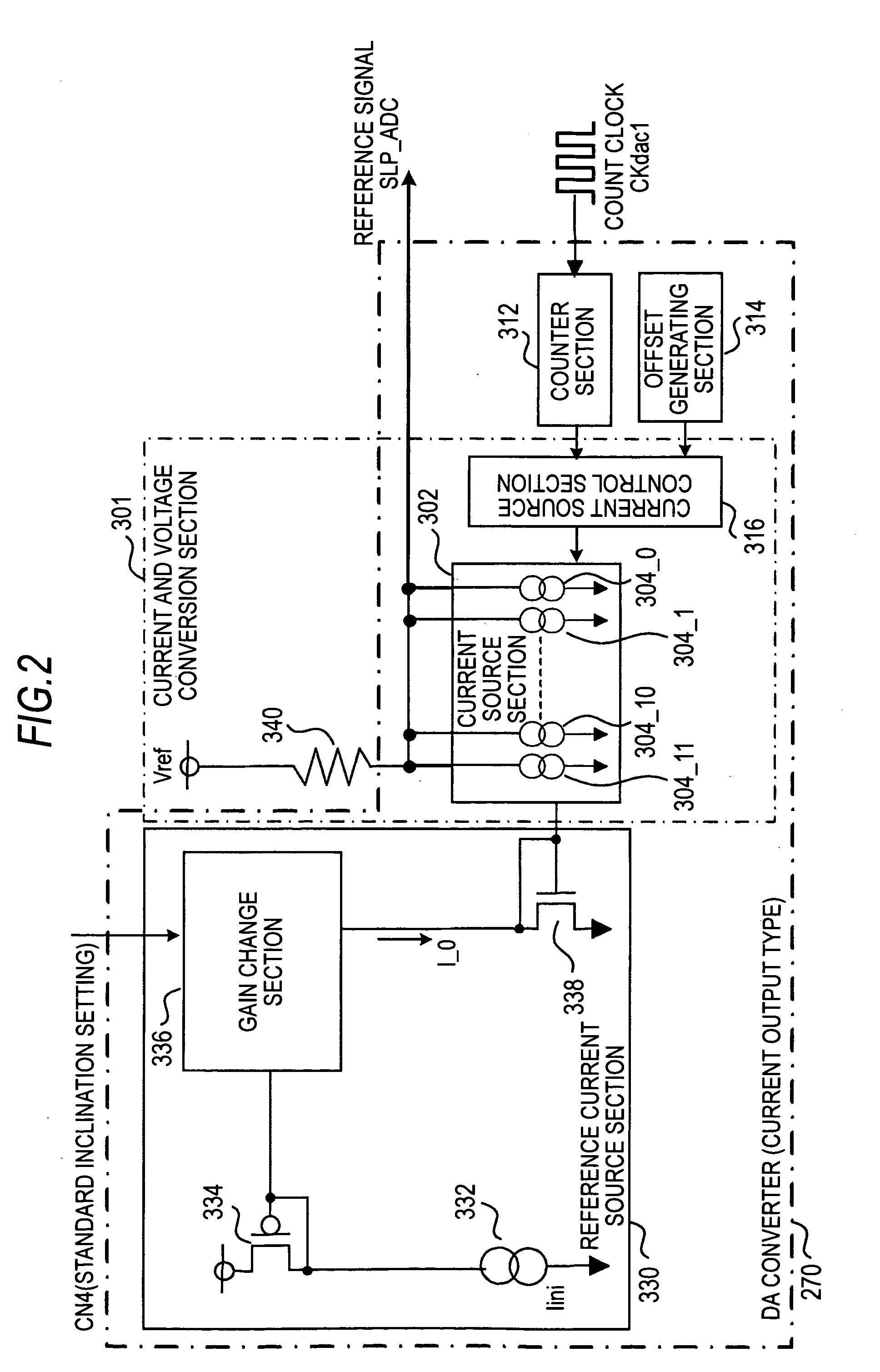
[0221]FIGS. 5A to 5G are views showing a second embodiment. Here, FIG. 5A is a view showing the simple circuit configuration of a solid state imaging device 1B according to the second embodiment when AD conversion processing and CDS processing are taken into consideration. FIG. 5B is a view showing an example of the configuration of a counter section used in the solid state imaging device according to the second embodiment. FIG. 5C is a view showing an example of the configuration of the reference signal generating section 27 (DA converter 270B) used in the solid state imaging device 1B according to the second embodiment. FIGS. 5D to 5F are views showing the details of the count operation period control section 253 in the second embodiment. FIG. 5D shows an example of the configuration, and FIGS. 5E and 5F are views showing an operation. FIG. 5G is a timing chart illustrating double AD conversion operations in the solid state imaging device 1B according to the second embodiment.
[022...
third embodiment
[0258]FIG. 6 is a timing chart illustrating double AD conversion operations in a solid state imaging device 1C according to a third embodiment. The configuration of the solid state imaging device 1C may be the same as that of the solid state imaging device 1A according to the first embodiment or the solid state imaging device 1B according to second embodiment. Here, the solid state imaging device 1C which has the same configuration as the solid state imaging device 1B according to the second embodiment is used.
[0259]In the third embodiment, AD processing is performed twice similar to the processing shown in FIG. 3E. Although the reference signal SLP_ADC with the same inclination (step width ΔSLP) is used in first and second AD conversion, the frequency of the count clock CKcnt1 that the counter section 254 uses is changed in the first and second AD conversion. The AD conversion resolution (number of bits) in the first and second processing is changed by changing the clock frequency ...
PUM
 Abstract
Description
Claims
Application Information
 - R&D Engineer
- R&D Manager
- IP Professional
- Industry Leading Data Capabilities
- Powerful AI technology
- Patent DNA Extraction
Browse by: Latest US Patents, China's latest patents, Technical Efficacy Thesaurus, Application Domain, Technology Topic.
© 2024 PatSnap. All rights reserved.Legal|Privacy policy|Modern Slavery Act Transparency Statement|Sitemap