Integrated circuit package-in-package system with side-by-side and offset stacking and method for manufacturing thereof
a technology of integrated circuits and packaging, which is applied in the direction of electrical equipment, semiconductor devices, semiconductor/solid-state device details, etc., can solve the problems of increasing manufacturing costs, unable to fully address the requirements of lower height, cost reduction, and small space, and existing packaging technologies cannot cost effectively meet the ever-demanding integration of integrated circuits and packages
- Summary
- Abstract
- Description
- Claims
- Application Information
AI Technical Summary
Benefits of technology
Problems solved by technology
Method used
Image

Examples
first embodiment
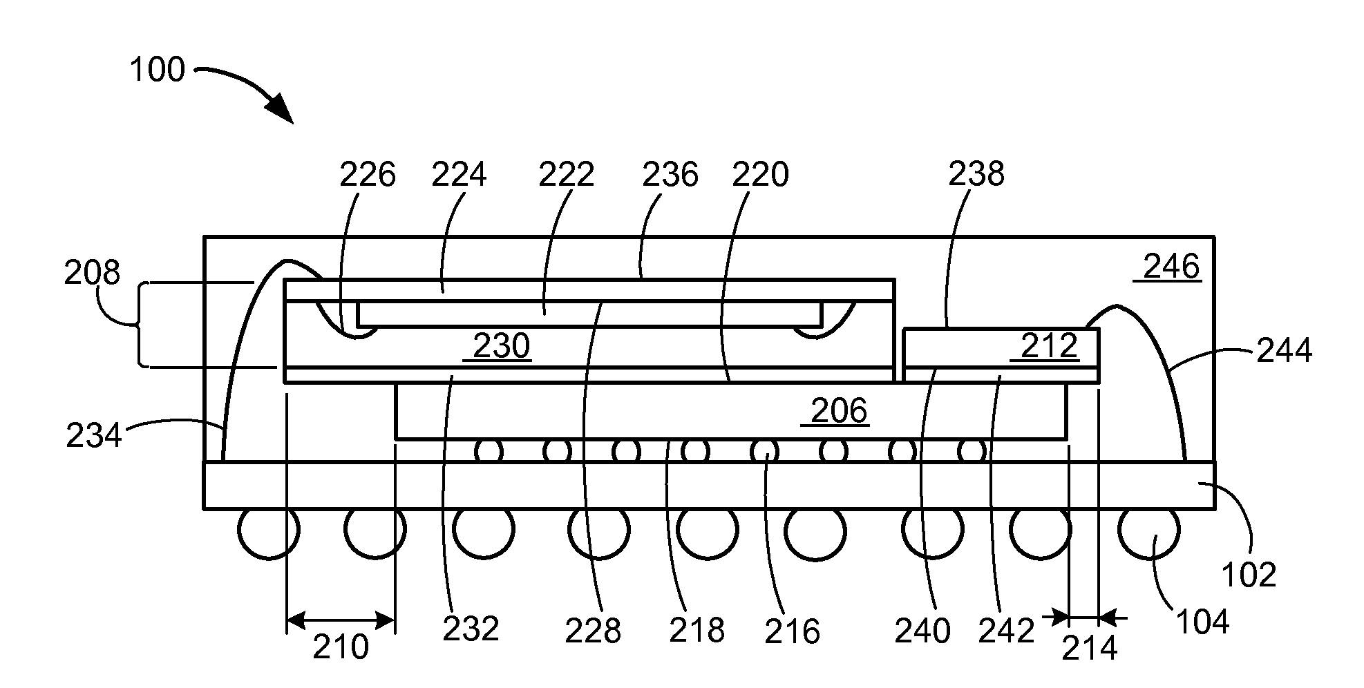
[0024]Referring now to FIG. 1, therein is shown a bottom view of an integrated circuit package-in-package system 100 in the present invention. The bottom view depicts a substrate 102, such as a laminated plastic or ceramic substrate, with external interconnects 104, such as solder balls, preferably attached to the substrate 102. For illustrative purposes, the external interconnects 104 are shown in an array configuration, although it is understood that the external interconnects 104 may populate the substrate 102 in a different configuration. For example, the external interconnects 104 may not populate all the locations of the array configuration.
[0025]Referring now to FIG. 2, therein is shown a cross-sectional view of the integrated circuit package-in-package system 100 along line 2-2 of FIG. 1. As described earlier, the external interconnects 104 are preferably attached below the substrate 102. A first integrated circuit device 206 preferably mounts over the substrate 102. An inte...
second embodiment
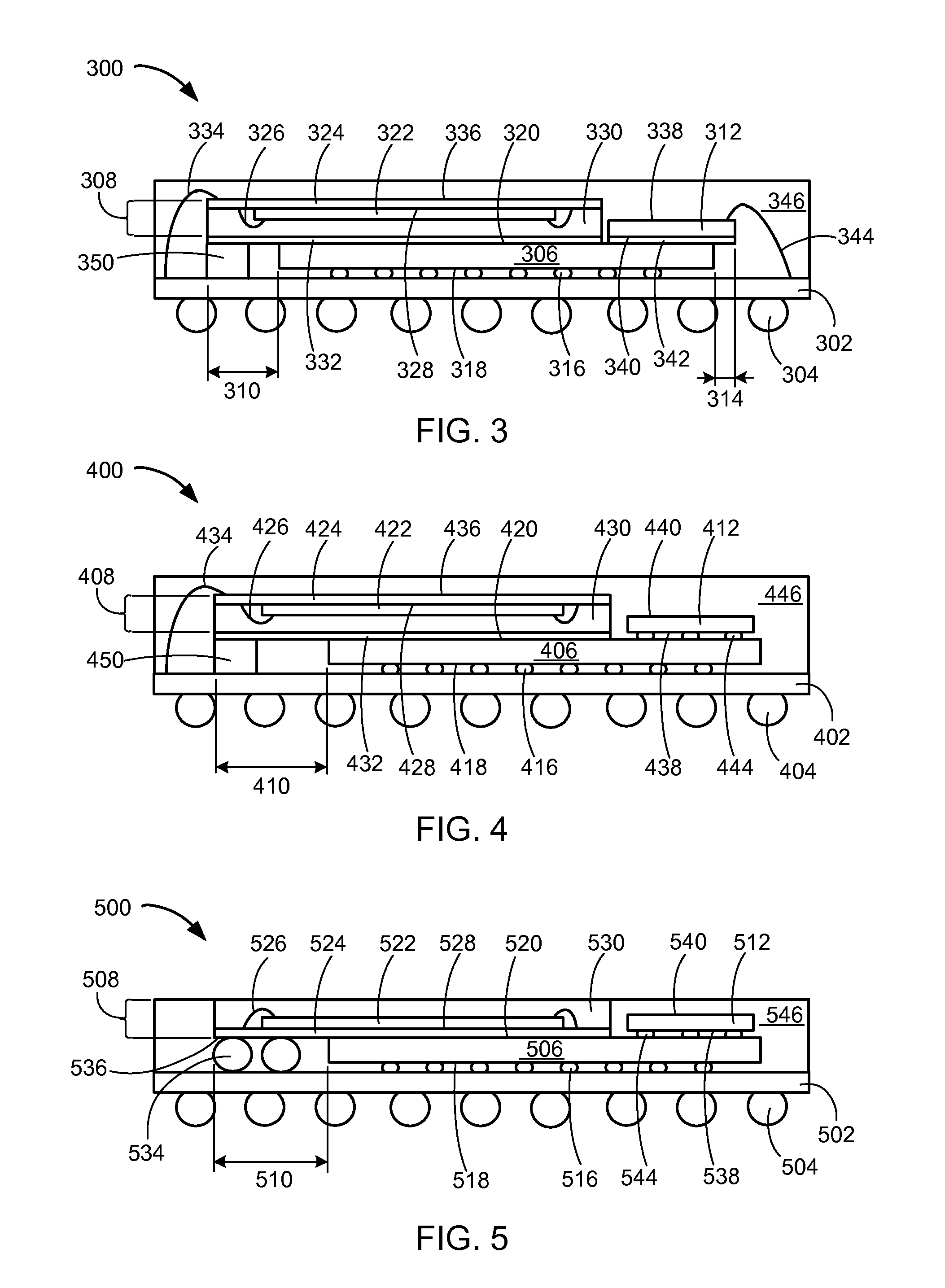
[0031]Referring now to FIG. 3, therein is shown a cross-sectional view of an integrated circuit package-in-package system 300 exemplified by the top view of FIG. 1 in the present invention. External interconnects 304, such as solder balls, are preferably attached below a substrate 302, such as a plastic or ceramic substrate. A first integrated circuit device 306 preferably mounts over the substrate 302. An integrated circuit package system 308 preferably mounts over the first integrated circuit device 306, wherein the integrated circuit package system 308 is shown, as an example, with a first offset 310 from the edge of the first integrated circuit device 306. A second integrated circuit device 312 is preferably adjacent, such as side-by-side, to the integrated circuit package system 308 and over the first integrated circuit device 306. The second integrated circuit device 312 is shown, as an example, with a second offset 314 from a different edge of the first integrated circuit dev...
third embodiment
[0038]Referring now to FIG. 4, therein is shown a cross-sectional view of an integrated circuit package-in-package system 400 exemplified by the top view of FIG. 1 in the present invention. External interconnects 404, such as solder balls, are preferably attached below a substrate 402, such as a plastic or ceramic substrate. A first integrated circuit device 406 preferably mounts over the substrate 402. An integrated circuit package system 408 preferably mounts over the first integrated circuit device 406, wherein the integrated circuit package system 408 is shown, as an example, with a first offset 410 from the edge of the first integrated circuit device 406. A second integrated circuit device 412 is preferably adjacent, such as side-by-side, to the integrated circuit package system 408 and over the first integrated circuit device 406.
[0039]As additional description to this example, the first integrated circuit device 406 is shown as a flip chip having electrical connectors 416, su...
PUM
 Abstract
Description
Claims
Application Information
 - R&D
- Intellectual Property
- Life Sciences
- Materials
- Tech Scout
- Unparalleled Data Quality
- Higher Quality Content
- 60% Fewer Hallucinations
Browse by: Latest US Patents, China's latest patents, Technical Efficacy Thesaurus, Application Domain, Technology Topic, Popular Technical Reports.
© 2025 PatSnap. All rights reserved.Legal|Privacy policy|Modern Slavery Act Transparency Statement|Sitemap|About US| Contact US: help@patsnap.com