Check patentability & draft patents in minutes with Patsnap Eureka AI!

Nonvolatile semiconductor memory device and method of manufacturing the same

a semiconductor memory and non-volatile technology, applied in the direction of semiconductor devices, basic electric elements, electrical appliances, etc., can solve the problems of aluminum oxide not improving the retention characteristics, the charge trap site density may not be sufficient inside the silicon nitride layer, and the paralytic capacitance may increase between neighboring gate stacks

Inactive Publication Date: 2010-12-23
SHIN SANG MIN +2
View PDF7 Cites 9 Cited by
  • Summary
  • Abstract
  • Description
  • Claims
  • Application Information

AI Technical Summary

Benefits of technology

The solution improves data retention characteristics by enhancing charge trap site density and thermal stability, allowing for longer retention times and faster programming and erasing speeds.

Problems solved by technology

Because a conventional flash semiconductor memory device may use a conductive material, for example, polysilicon doped with a floating gate material, parasitic capacitance may increase between neighboring gate stacks when the device is highly integrated.
However, although the blocking insulating layer formed of aluminum oxide may suppress charges moving from the silicon nitride layer to an extent, the charge trap site density inside the silicon nitride layer may still not be sufficient.
As such, the retention characteristics may not be improved by the aluminum oxide.
Thus, it may be difficult to obtain sufficient retention time using a conventional silicon nitride layer.

Method used


Image

  • Nonvolatile semiconductor memory device and method of manufacturing the same
  • Nonvolatile semiconductor memory device and method of manufacturing the same
  • Nonvolatile semiconductor memory device and method of manufacturing the same

Examples


Embodiment Construction

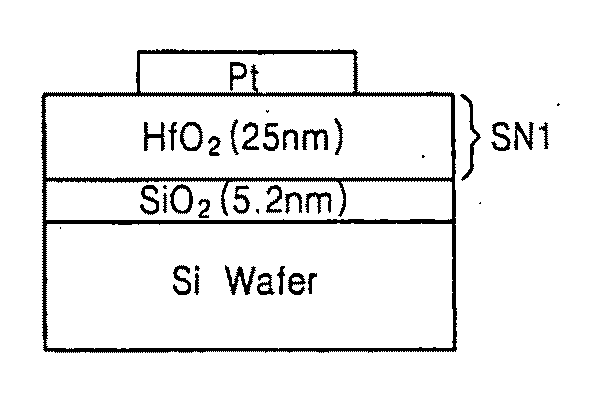
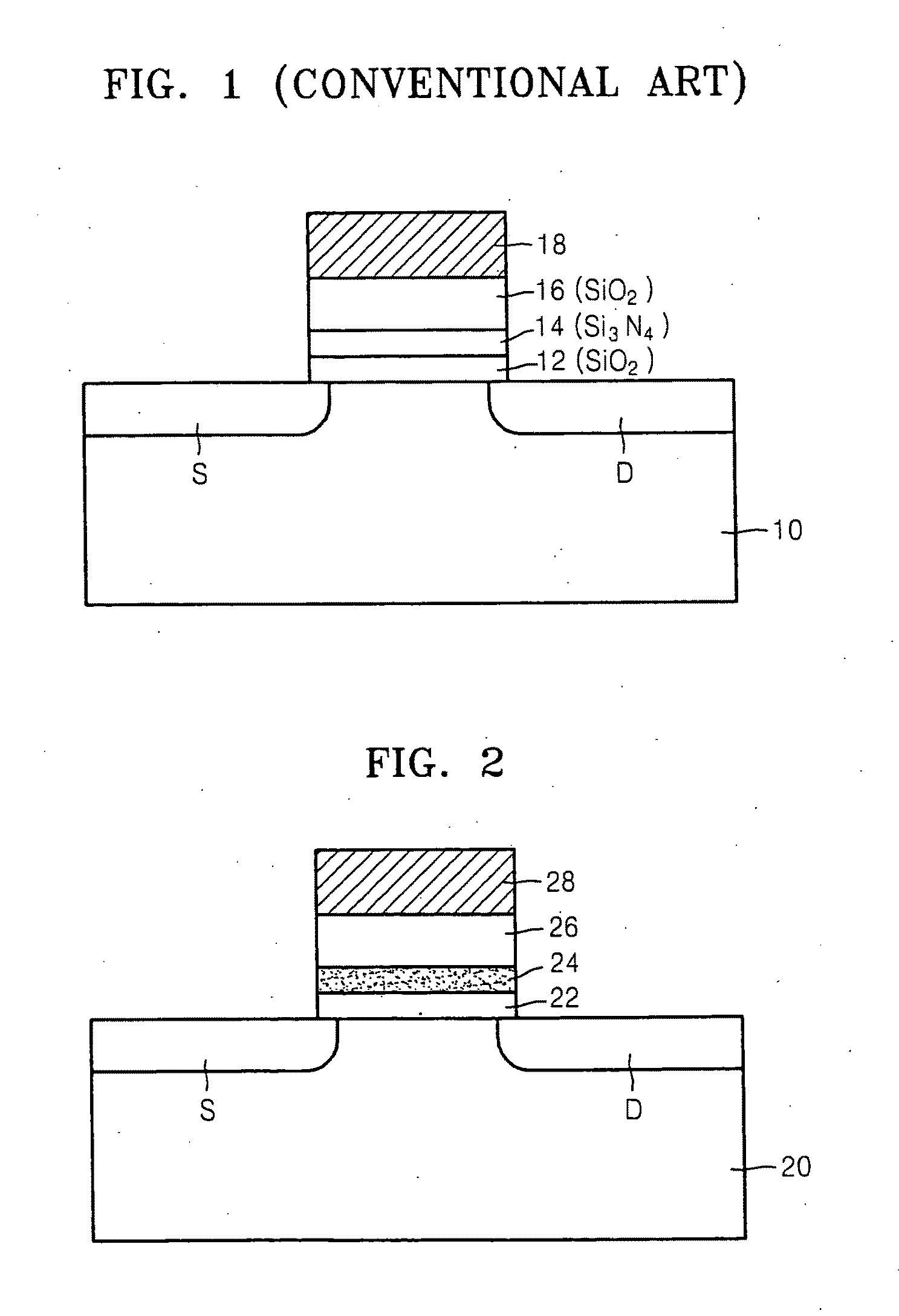
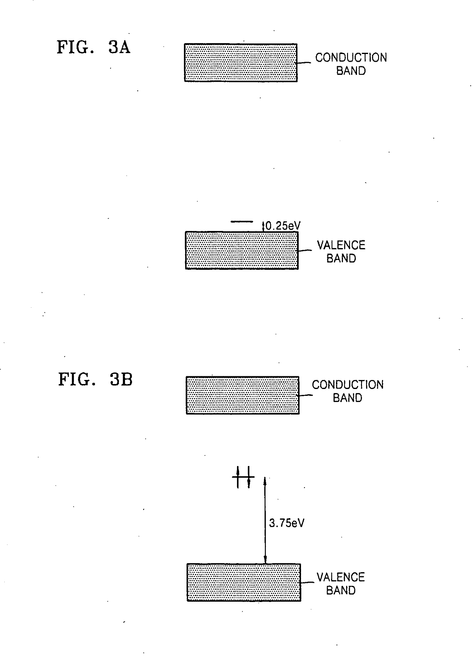
[0045]Reference will now be made in detail to example embodiments, examples of which are illustrated in the accompanying drawings. However, example embodiments are not limited to the embodiments illustrated hereinafter, and the embodiments herein are rather introduced to provide easy and complete understanding of the scope and spirit of example embodiments. In the drawings, the thicknesses of layers and regions are exaggerated for clarity.

[0046]It will be understood that when an element or layer is referred to as being “on,”“connected to” or “coupled to” another element or layer, it may be directly on, connected or coupled to the other element or layer or intervening elements or layers may be present. In contrast, when an element is referred to as being “directly on,”“directly connected to” or “directly coupled to” another element or layer, there are no intervening elements or layers present. Like reference numerals refer to like elements throughout. As used herein, the term “and / or...


PUM


Abstract

Provided is a nonvolatile semiconductor memory device and a method of manufacturing the same. The nonvolatile semiconductor memory device may include a tunnel insulating layer formed on a semiconductor substrate, a charge trap layer including a dielectric layer doped with a transition metal formed on the tunnel insulating layer, a blocking insulating layer formed on the charge trap layer, and a gate electrode formed on the blocking insulating layer. The dielectric layer may be a high-k dielectric layer, for example, a HfO2 layer. Thus, the data retention characteristics of the nonvolatile semiconductor memory device may be improved because a deeper charge trap may be formed by doping the high-k dielectric layer with a transition metal.

Description

PRIORITY STATEMENT[0001]This U.S. nonprovisional application is a divisional of U.S. application Ser. No. 11 / 723,081, filed Mar. 16, 2007 and claims priority under 35 USC §121 to Korean Patent Application No. 2006-0070886, filed on Jul. 27, 2006, in the Korean Intellectual Property Office (KIPO), the entire contents of which are herein incorporated by reference.BACKGROUND[0002]1. Field[0003]Example embodiments relate to a nonvolatile semiconductor memory device with improved data retention characteristics and method of manufacturing the same.[0004]2. Description of the Related Art[0005]Nonvolatile semiconductor memory devices capable of storing data, erasing data electrically, and retaining stored data when power is removed have been a source of much interest.[0006]The characteristics of a memory cell of a nonvolatile semiconductor memory device may vary according to the field in which the nonvolatile semiconductor memory device is used. For example, the gate stack of a transistor o...

Claims


Application Information

Patent Timeline
Patent Type & Authority Applications(United States)
IPC IPC(8): H01L21/283H10B69/00
CPCH01L21/28282H01L29/42332H01L29/792H01L29/513H01L29/7881H01L29/42348H01L29/40117H01L29/66833
Inventor SHIN, SANG-MINSEOL, KWANG-SOOJIN, YOUNG-GU
Owner SHIN SANG MIN
Features
  • R&D
  • Intellectual Property
  • Life Sciences
  • Materials
  • Tech Scout
  • Unparalleled Data Quality
  • Higher Quality Content
  • 60% Fewer Hallucinations
Learn More