
Compound for organic thin film transistor and organic thin film transistor using the same

a technology of organic thin film transistors, applied in the direction of organic chemistry, chemistry apparatus and processes, thermoelectric devices, etc., can solve the problems of high production cost, use as a substrate, and high cost of cvd apparatus used for fabricating tft using silicon, so as to improve film-forming properties and high mobility

Inactive Publication Date: 2011-09-15
IDEMITSU KOSAN CO LTD
View PDF2 Cites 11 Cited by
  • Summary
  • Abstract
  • Description
  • Claims
  • Application Information

AI Technical Summary

Benefits of technology

[0012]The invention is aimed at providing a compound for an organic thin film transistor which is excellent in film-forming properties. The invention is also aimed at providing an organic thin film transistor which has a high mobility.
[0019]According to the invention, a compound for an organic thin film transistor improved in film-forming properties or an organic thin film transistor having a high mobility can be provided.

Problems solved by technology

However, a CVD apparatus which is used for fabricating a TFT using silicon is very expensive.
Therefore, there was a problem that an increase in size of a display apparatus or the like using a TFT resulted in a significant increase in production cost.
Further, since forming an amorphous or polycrystalline silicon into a film is conducted at a significantly high temperature, kind of materials which can be used as a substrate is limited, which makes the use of a light-weight resin substrate or the like impossible.
However, the above-mentioned compounds used in conventional organic TFTs have a small field effect mobility and a slow response speed, and hence, the high-speed responsiveness thereof as a transistor is not satisfactory.
This organic TFT has a defect that, though it exhibits a significantly high mobility immediately after the fabrication of a device, pentacene has a low stability in an atmosphere.

Method used


Image

  • Compound for organic thin film transistor and organic thin film transistor using the same
  • Compound for organic thin film transistor and organic thin film transistor using the same
  • Compound for organic thin film transistor and organic thin film transistor using the same

Examples


example 1

Synthesis of Compound (1)

[0123]The compound (1) was synthesized as follows.

Sandmeyer Reaction

[0124]

[0125]To a reactor, 400 ml of an acetonitrile solution of 44.2 g (198 mmol) of copper (II) bromide and 20.4 g (198 mmol) of tert-butyl nitrite was added. 29.7 g (82.5 mmol) of 3,6-diiodo-1,2-diaminebenzene was gradually added thereto, and the reactor was refluxed with heating at 65° C. for 3 hours. After the reaction mixture was cooled to room temperature, 200 ml of 20% hydrochloric acid was added. An organic layer was extracted with ether, and dried with magnesium sulfate. The resulting filtrate was concentrated, whereby 5.53 g (yield: 14%) of dibromodiiodobenzene was obtained.

[0126]62 ml of a dimethoxy ether solution of 5.0 g (10.3 mmol) of dibromodiiodobenzene, 0.60 g (0.515 mmol) of tetraxistriphenylphosphine palladium (0) and 2.8 g (20.6 mmol) of 4-methylphenylboronic acid were placed in a reactor. 31 ml of an aqueous 2M sodium carbonate solution was added thereto, and the reactor...

example 2

Production of an Organic Thin Film Transistor

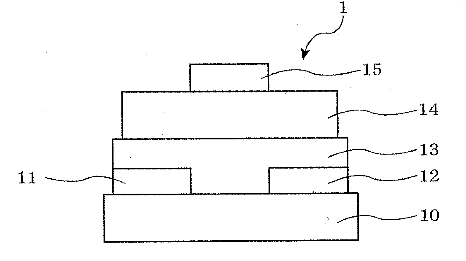
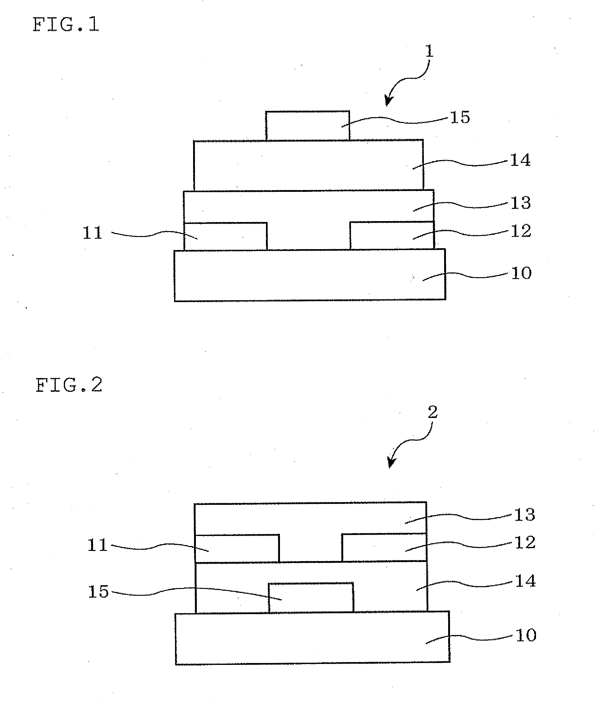
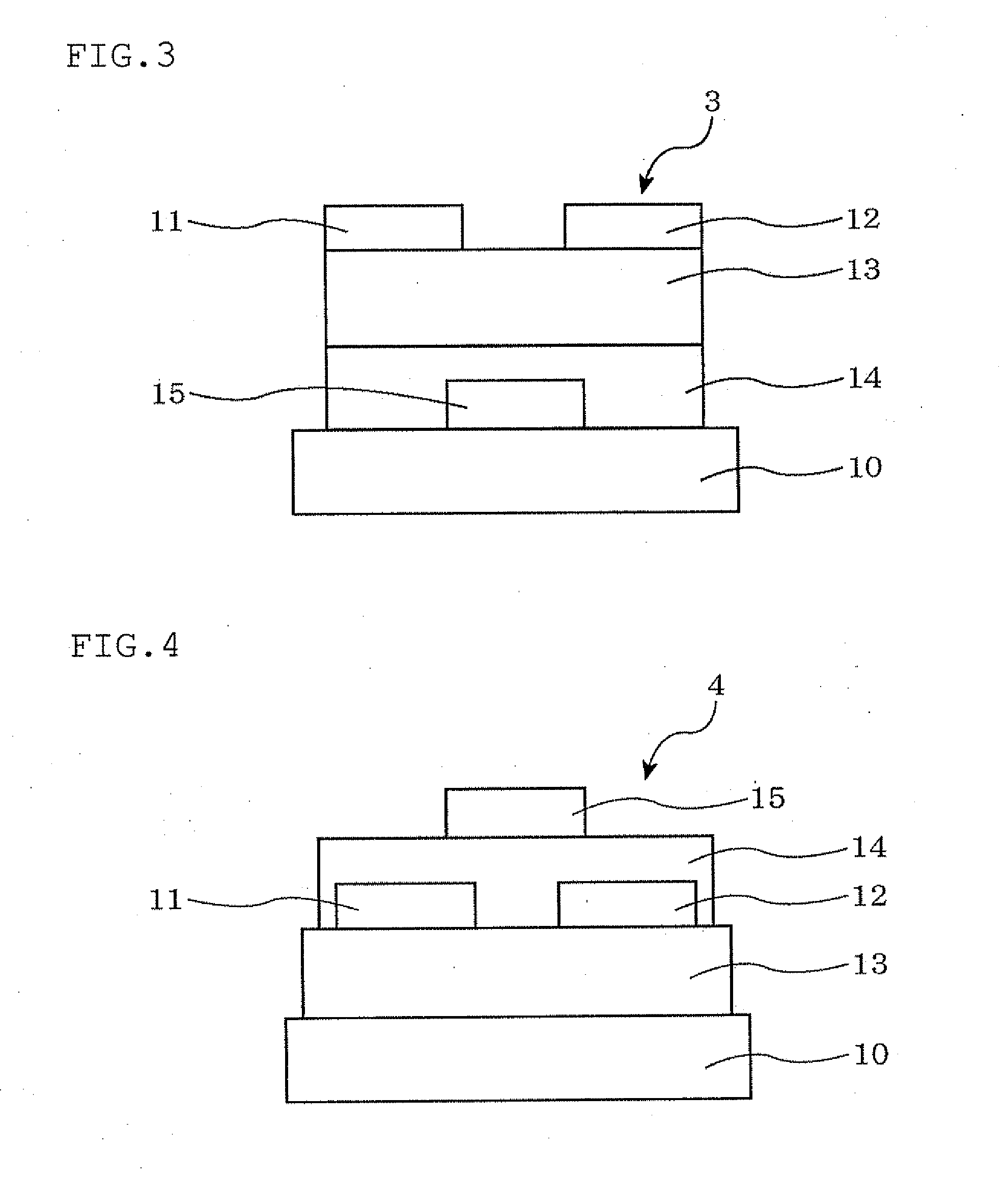
[0140]An organic thin film transistor was manufactured through the following steps. First, the surface of an Si substrate (also served as a p-type gate electrode with a specific resistance of 1 Ωcm) was oxidized by the thermal oxidation method, whereby a 300 nm-thick thermally oxidized film was formed on the substrate to form an insulator layer. Further, an SiO2 film formed on one side of the substrate was completely removed by dry etching, and thereafter, chromium was formed into a film of 100 nm by the sputtering method. Further, gold (Au) was formed thereon into a film of 100 nm by the sputtering method, whereby an outcoupling electrode was formed. This substrate was subjected to ultrasonic cleaning for 30 minutes each with a neutral detergent, pure water, acetone and ethanol. The substrate was further subjected to ozone cleaning.

[0141]The substrate was then subjected to a surface treatment by heating for 3 hours in the atmosphere of h...

examples 3 to 7

Synthesis of Compounds (8), (12), (13), (14) and (50)

[0144]Compounds (8), (12), (13), (14) and (50) were obtained in the same manner as in Example 1, except that 4-methylboronic acid used in the synthesis of the compound (A) in Examples 1 was changed to a boronic acid derivative corresponding to each compound.

[0145]Further, compounds (8), (12), (13) and (14) were

synthesized in the same manner as Example 1, except that, in the synthesis of the compound (D), N-(4-alkylcyclohexylidene)cyclohexanamine corresponding to each compound was used.

[0146]As a result of the measurement by FD-MS (field desorption mass spectrometry), the compounds were confirmed to be intended products. The measurement results of FD-MS are given below.

Compound (8)

[0147]FD-MS, calcd for C38H46=502. Found, m / z=502 (M+, 100).

Compound (12)

[0148]FD-MS, calcd for C46H62=614. Found, m / z=614 (M+, 100).

Compound (13)

[0149]FD-MS, calcd for C48H66=642. Found, m / z=642 (M+, 100).

Compound (14)

[0150]FD-MS, calcd for C50H70=670. F...


PUM

PropertyMeasurementUnit
work functionaaaaaaaaaa
thicknessaaaaaaaaaa

Abstract

A compound for an organic thin film transistor having a structure of the following formula (1):wherein R1 to R6 are independently a hydrogen atom, a halogen atom, an alkyl group having 1 to 30 carbon atoms, a haloalkyl group having 1 to 30 carbon atoms, an alkoxy group having 1 to 30 carbon atoms, a haloalkoxy group having 1 to 30 carbon atoms, an alkylthio group having 1 to 30 carbon atoms, a haloalkylthio group having 1 to 30 carbon atoms, an alkylamino group having 1 to 30 carbon atoms, a dialkylamino group having 2 to 60 carbon atoms (the alkyl groups may be combined with each other to form a ring structure containing the nitrogen atom), an alkylsulfonyl group having 1 to 30 carbon atoms, a haloalkylsulfonyl group having 1 to 30 carbon atoms, an aromatic hydrocarbon group having 6 to 60 carbon atoms, an aromatic heterocyclic group having 3 to 60 carbon atoms, an alkylsilyl group having 3 to 20 carbon atoms, an alkylsilylacetylene group having 5 to 60 carbon atoms or a cyano group, which each may have a substituent, provided that the compound in which all of R1 to R6 are a hydrogen atom is excluded.

Description

TECHNICAL FIELD[0001]The invention relates to a compound for an organic thin film transistor and an organic thin film transistor using it in an organic semiconductor layer.BACKGROUND ART[0002]A thin film transistor (TFT) has been used widely as a switching device for a display of a liquid crystal display apparatus or the like. A representative TFT comprises a gate electrode, an insulating layer and an organic semiconductor layer sequentially on a substrate, and a source electrode and a drain electrode formed on the organic semiconductor layer with a predetermined interval. The organic semiconductor layer constitutes a channel region, and a TFT performs an on-off operation by adjusting current flowing between the source electrode and the drain electrode by a voltage applied to the gate electrode.[0003]Conventionally, a TFT was fabricated by using amorphous or polycrystalline silicon. However, a CVD apparatus which is used for fabricating a TFT using silicon is very expensive. Therefo...

Claims


Application Information

Patent Timeline
Patent Type & Authority Applications(United States)
IPC IPC(8): H01L51/52H01L51/10C07C13/62C07C43/20C07C321/26C07C317/14C07C211/50C07D207/04C07C25/13C07C22/04C07C255/52
CPCC07C15/20C07C43/2055C07C2103/52H01L51/0558H01L51/0541H01L51/0545H01L51/0055C07C2603/52H10K85/623H10K10/464H10K10/484H10K10/466H10K10/84
Inventor NAKANO, YUKISAITO, MASATOSHINAKAMURA, HIROAKI
Owner IDEMITSU KOSAN CO LTD
Learn More