Method of fabricating a semiconductor device including ion implantation at a tilt angle in exposed regions
a technology of exposed regions and semiconductors, applied in the direction of semiconductor devices, basic electric elements, electrical equipment, etc., can solve the problems of adversely affecting the production yield of the device, the inability to simultaneously activate left and right transistors, and the significant deterioration of the device characteristics
- Summary
- Abstract
- Description
- Claims
- Application Information
AI Technical Summary
Benefits of technology
Problems solved by technology
Method used
Image

Examples
Embodiment Construction
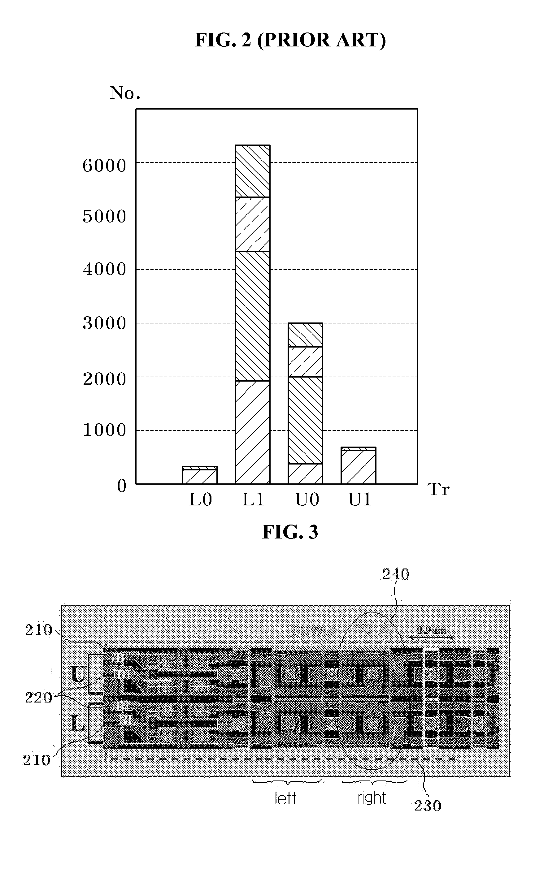
[0029]The present invention examines the cause of mismatched transistors included in a sense amplifier and provides a method of solving problems associated with the mismatch. In order to examine the cause of the mismatch, the mask layout of the sense amplifier will be described.
[0030]FIG. 3 is a view showing a mask layout of a sense amplifier.
[0031]Four transistors are symmetrically provided between a pair of bit lines BL (210) and / BL (220). In particular, two left transistors are spaced from the edge of a P-well 230 by at least a predetermined distance, and two right transistors are spaced from the edge of the P-well 230 by about 0.9 μm.
[0032]As shown in FIG. 2, the bump failure rate of the two right transistors 240 is larger than that of the two left transistors. Accordingly, the bump failure rate is associated with the distance between the transistor and the P-well.
[0033]In order to fabricate a semiconductor memory device, a variety of processes including a laminating process, a...
PUM
 Abstract
Description
Claims
Application Information
 - R&D
- Intellectual Property
- Life Sciences
- Materials
- Tech Scout
- Unparalleled Data Quality
- Higher Quality Content
- 60% Fewer Hallucinations
Browse by: Latest US Patents, China's latest patents, Technical Efficacy Thesaurus, Application Domain, Technology Topic, Popular Technical Reports.
© 2025 PatSnap. All rights reserved.Legal|Privacy policy|Modern Slavery Act Transparency Statement|Sitemap|About US| Contact US: help@patsnap.com