
Night vision CMOS imager with optical pixel cavity

a cmos imager and optical pixel technology, applied in the field of imaging devices, can solve the problems of intensifier tubes, high cost, large size and high cost, and achieve the effect of low cost, small size and low cost of cmos imaging devices

Active Publication Date: 2012-03-01
SRI INTERNATIONAL
View PDF16 Cites 24 Cited by
  • Summary
  • Abstract
  • Description
  • Claims
  • Application Information

AI Technical Summary

Benefits of technology

[0016]According to an embodiment of the present invention, a distance between the first reflective layer and the second reflective layer may be lar

Problems solved by technology

Reasons for replacing intensifier tubes include their large size and high cost.
In contrast, CMOS imaging devices are of generally low cost and small size, have direct electronic output, and have a potentially higher mean time between failures (MTF).
Unfortunately, conventional CMOS imagers cannot match the low light performance of intensifier tubes because room temperature dark current is too high for devices thick enough to have high near infra-red (IR) quantum efficient (QE) needed for night vision.
Unfortunately, the lowest possible dark current limit results from bulk silicon.
Unfortunately, but the absorption region for photons in such devices is too thin to have high QE at near IR wavelengths needed for night vision.
Unfortunately, there is no discussion of silicon volume in the '326 patent.
Therefore, the bulk silicon dark current issue remains.

Method used


Image

  • Night vision CMOS imager with optical pixel cavity
  • Night vision CMOS imager with optical pixel cavity
  • Night vision CMOS imager with optical pixel cavity

Examples


Embodiment Construction

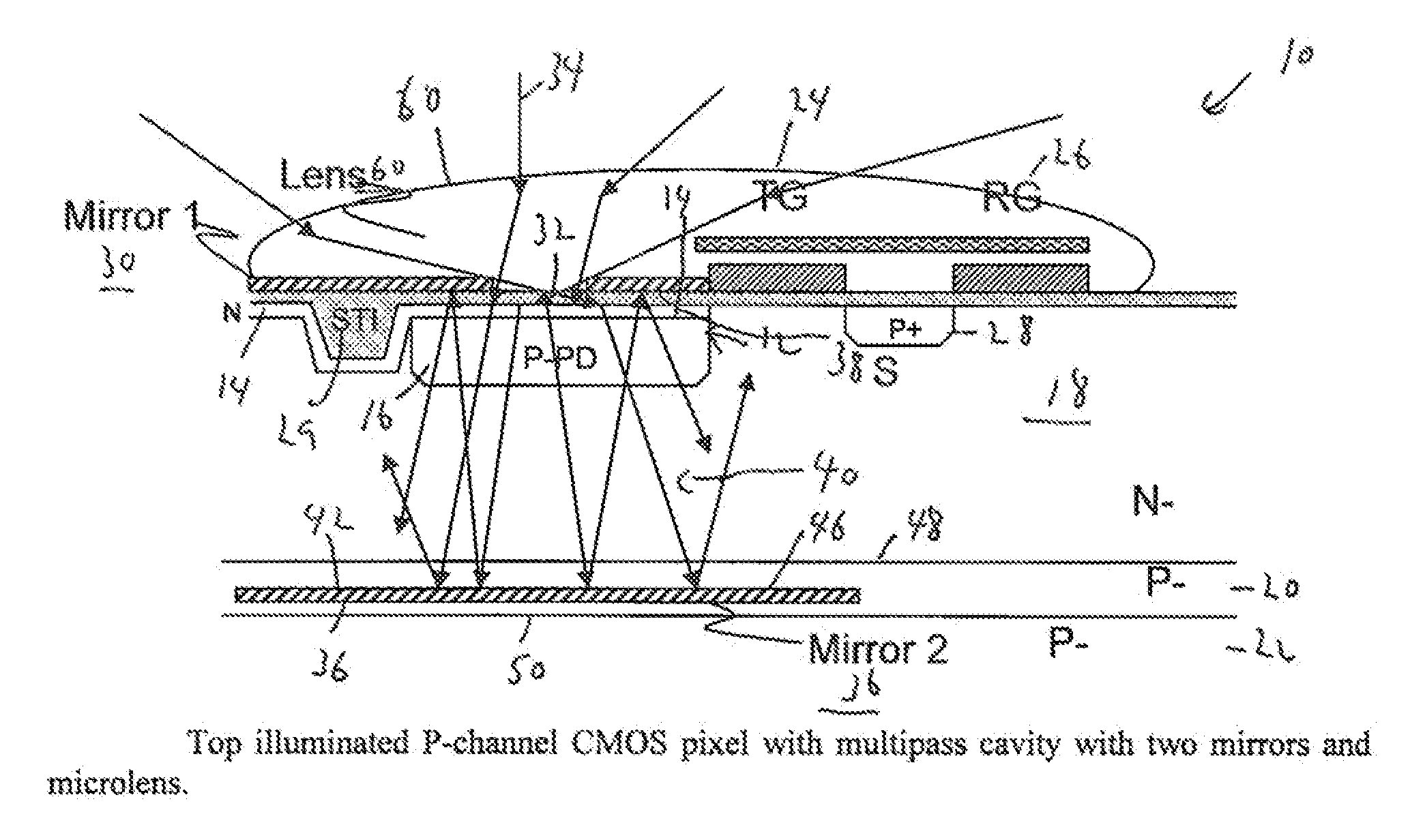
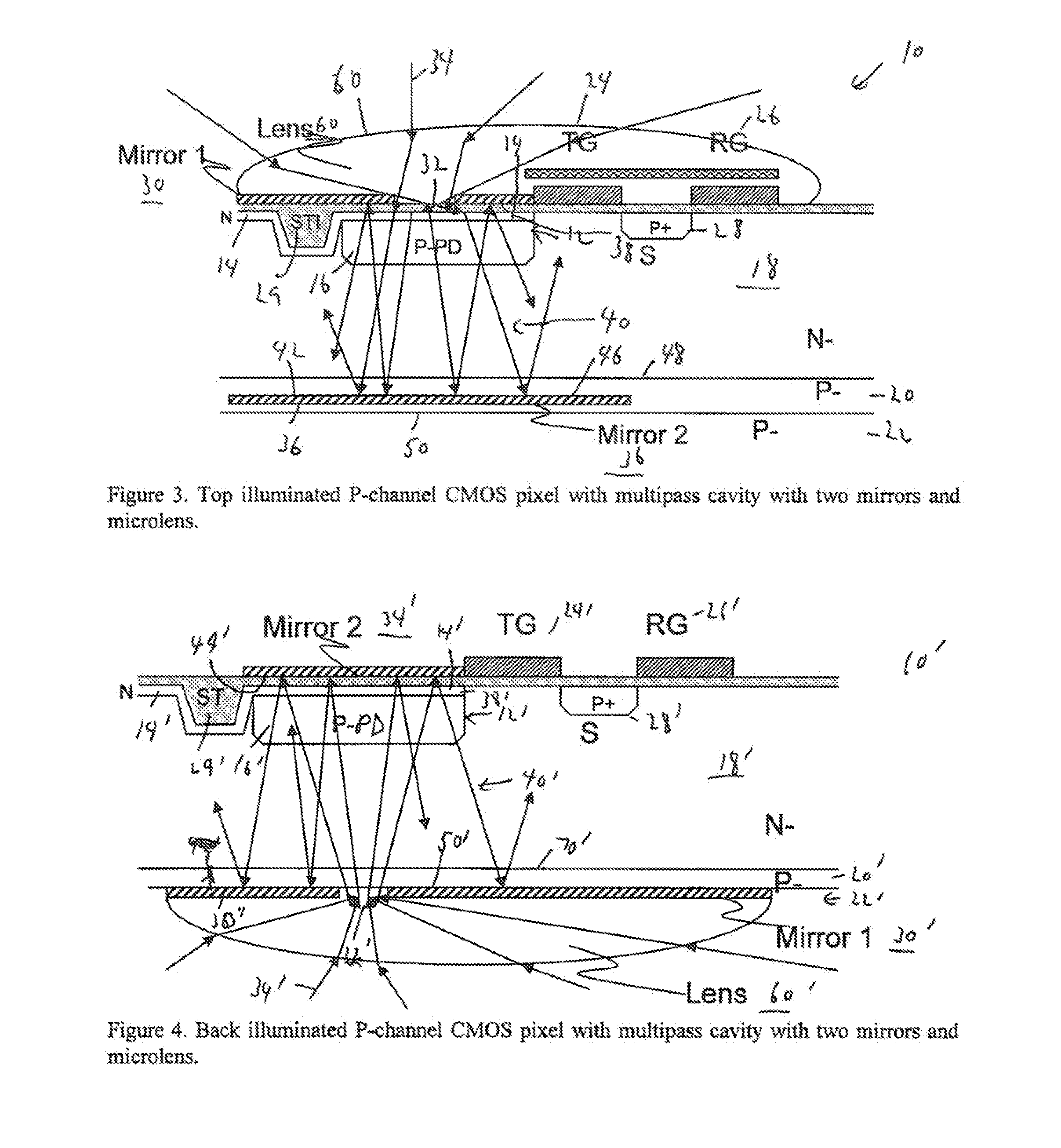
[0025]Certain embodiments of the present invention pertain to pixel designs. A pixel comprising a small volume of detecting silicon contained in an optical cavity that provides multiple light passes through the detecting silicon over a wide range of wavelengths. The optical cavity may be formed by flat or curved minors to reduce pixel-to-pixel cross-talk and improve QE. The optical cavity is effectively non-resonant with respect to photon absorption because the thickness of the silicon is large compared to the wavelength of light being detected.

[0026]An aperture is provided in one of the minors for light to enter the cavity. The shape of the mirrors may be curved to minimize loss of light reflected back to the aperture and reduce cross talk between pixels. Each pixel may have an associated microlens capable of focusing light falling on the lens area to a small spot which fits within the cavity aperture to improve QE. In an embodiment, the diameter of the aperture is significantly sm...


PUM


Abstract

A pixel design is disclosed. The pixel includes a photo-sensitive element. A first reflective layer substantially overlies the photo-sensitive element. A second reflective layer substantially underlies the photo-sensitive element and forms a cavity with the first reflective layer that is non-resonant with respect to photon absorption. An aperture is formed in either the first reflective layer or the second reflective layer. When electromagnetic radiation enters the aperture, the first reflective layer and the second reflective layer are configured to reflect the electromagnetic radiation substantially toward each other until substantially absorbed in the cavity.

Description

CROSS-REFERENCE TO RELATED APPLICATION[0001]This application claims the benefit of U.S. provisional patent application No. 61 / 376,758 filed Aug. 25, 2010, the disclosure of which is incorporated herein by reference in its entirety.FIELD OF THE INVENTION[0002]The invention relates generally to imaging devices. More specifically, the invention relates to CMOS charge transfer pixels for night vision applications.BACKGROUND OF THE INVENTION[0003]Generally, an image sensor is a semiconductor device for converting an optical image into an electric signal. There are a number of different types of semiconductor-based imagers, including charge coupled devices (CCDs), photodiode arrays, charge injection devices, hybrid focal plane arrays, etc. The various types of image sensors may be broadly categorized as charge coupled devices (CCD) and complementary metal oxide semiconductor (CMOS) image sensors.[0004]In recent years, there has also been increased interest in applying CMOS active pixel se...

Claims


Application Information

Patent Timeline
IPC IPC(8): H04N5/225
CPCH01L27/14609H01L27/14627H04N5/374H01L27/1464H04N5/33H01L27/14629H04N25/76
Inventor LEVINE, PETER ALANZHU, RUITOWER, JOHN ROBERTSON
Owner SRI INTERNATIONAL
Learn More