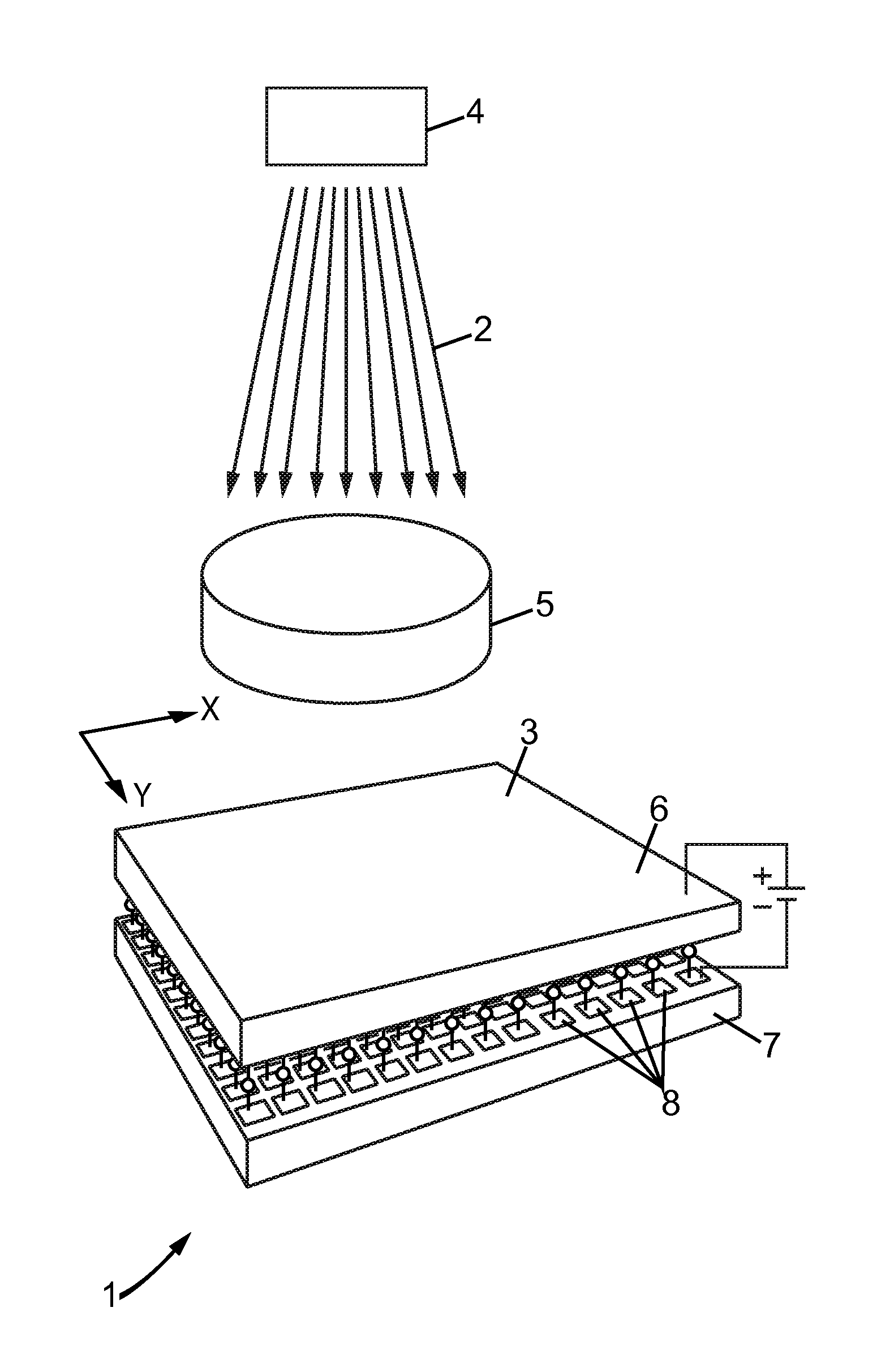
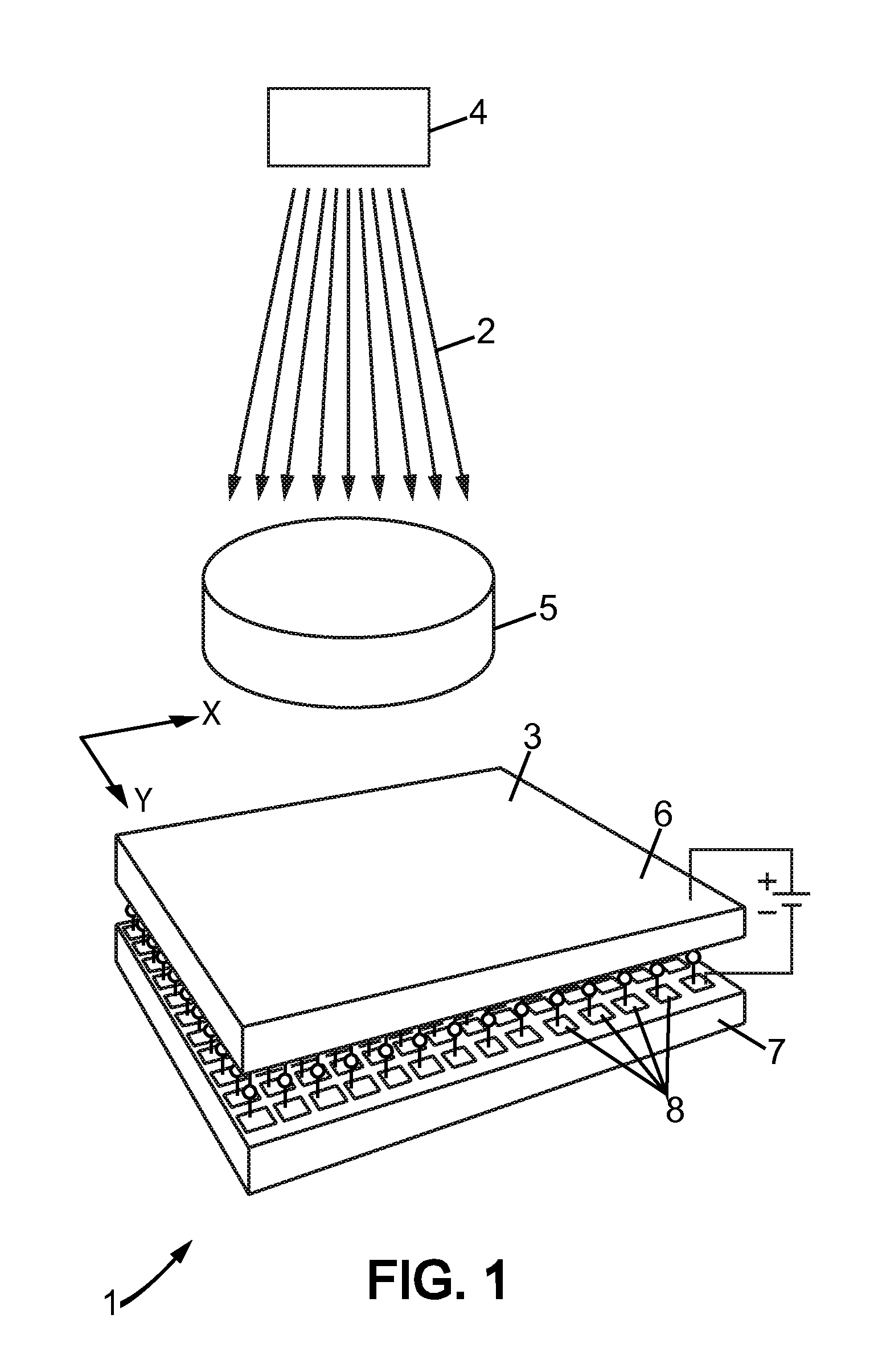
Pixilated radiation sensing device
- Summary
- Abstract
- Description
- Claims
- Application Information
AI Technical Summary
Problems solved by technology
Method used
Image

Examples
first embodiment
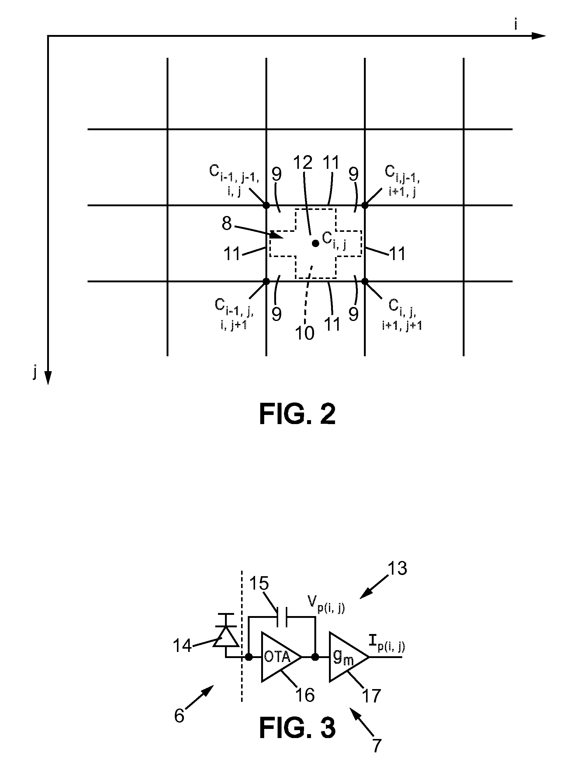
[0029]As shown below, on FIG. 2, a pixel 8 has n corner regions 9 (with in the present case, n=4), and a central region 10. The central region 10 is arbitrarily delimited by the dotted line on FIG. 2. It comprises all the part of the pixel, which is not in the corner regions 9. Further, the central region 10 has a centre 12, which approximately, is the centre of the pixel. as shown on FIG. 2, the electronic part comprises for each pixel five counters:[0030]counter Ci−1,j−1,i,j associated to the top left corner of FIG. 2,[0031]counter Ci,j−1,i+1,j associated to the top right corner of FIG. 2,[0032]counter Ci−1,j,i,j+1 associated to the bottom left counter of FIG. 2,[0033]counter Ci,j,i+1,j+1 associated to the bottom right corner of FIG. 2, and[0034]counter Ci,j associated to the central region.
[0035]For example, in the first embodiment Ci,j is associated to the centre 12 of the central region 10 of the pixel 8.
[0036]Hence, each of these counters is associated to a different region o...
second embodiment
[0091] the discriminating circuit 22 compares the four input signals and checks whether these signals are all substantially equal (the difference between the minimum and the maximum of these four signals being less than a predetermined threshold).
[0092]If the discriminating circuit 22 determines that the four inputs are substantially equal, it elects the counter Ci,j of the central region as the elected counter. Further, it allocates to the elected counter a detection value such as, for example, Ii,j. Further, it can also allocate a detection value of zero (0) to the counters associated to the corner regions.
[0093]To the contrary, if the discriminating circuit 22 determines that at least two of the four input are substantially different, it allocates zero to the counter Ci,j associated to the central region. In such cases, one of the corners associated to a corner region will be the elected counter. Determination of the elected counter is performed by the comparison circuit 20 as in...
third embodiment
[0098]FIG. 9 now shows the invention.
[0099]In this third embodiment, there is not necessarily a counter Ci,j associated to the centre of the central region 10 of the pixel. However, counters can be associated to edges 11 between two neighbour corner regions 9.
[0100]As explained above, these edge counters are each associated to the central region 10, the central region 10 including any part of the pixel which is not in the corners.
[0101]For example, as shown on FIG. 9, there are four edge counters:[0102]counter Ci,j−1,j associated to the top of the pixel,[0103]counter Ci−1,i,j associated to the left of the pixel,[0104]counter Ci,i+1,j associated to the right of the pixel, and[0105]counter Ci,j,j+1 associated to the bottom of the pixel.
[0106]Hence, as is the case for the counters associated to corner regions, which are each shared by four pixels, edge counters are shared by two pixels.
[0107]The regions associated to each counter are purely arbitrarily designated by dotted lines on FIG...
PUM
 Abstract
Description
Claims
Application Information
 - R&D Engineer
- R&D Manager
- IP Professional
- Industry Leading Data Capabilities
- Powerful AI technology
- Patent DNA Extraction
Browse by: Latest US Patents, China's latest patents, Technical Efficacy Thesaurus, Application Domain, Technology Topic.
© 2024 PatSnap. All rights reserved.Legal|Privacy policy|Modern Slavery Act Transparency Statement|Sitemap