Check patentability & draft patents in minutes with Patsnap Eureka AI!

Semiconductor chip having plural penetrating electrodes that penetrate therethrough

a technology of semiconductors and penetrating electrodes, applied in the direction of individual semiconductor device testing, semiconductor/solid-state device testing/measurement, instruments, etc., can solve the problem of large number of penetrating electrodes, inability to measure the resistance value of miniaturized penetrating electrodes using the four-terminal method, and disadvantageous increase in resistan

Inactive Publication Date: 2013-05-30
PS4 LUXCO SARL
View PDF3 Cites 4 Cited by
  • Summary
  • Abstract
  • Description
  • Claims
  • Application Information

AI Technical Summary

Benefits of technology

The present invention allows for accurate measurement of resistance values of penetrating electrodes in semiconductor chips, even when the size of the electrodes is reduced. This is achieved by providing a connection between each electrode and a separate terminal, regardless of the size of the electrodes. This ensures reliable and accurate measurement of the resistance values, allowing for improved performance and reliability of the semiconductor chip.

Problems solved by technology

However, the through Si conductors each formed to a thickness that does not fill the through hole) disclosed in Patent Documents 1 and 2 each have a cross-section area smaller than that of the through hole and are therefore disadvantageously increased in resistance.
Further, in a semiconductor device (semiconductor chip) exchanging a large number of signals with an external device through the penetrating electrode, a large number of the penetrating electrodes is required.
The following problem arises when the miniaturization of the through hole is progressed as described above.
That is, the resistance of the miniaturized penetrating electrode cannot be measured by using the four-terminal method.

Method used


Image

  • Semiconductor chip having plural penetrating electrodes that penetrate therethrough
  • Semiconductor chip having plural penetrating electrodes that penetrate therethrough
  • Semiconductor chip having plural penetrating electrodes that penetrate therethrough

Examples


first embodiment

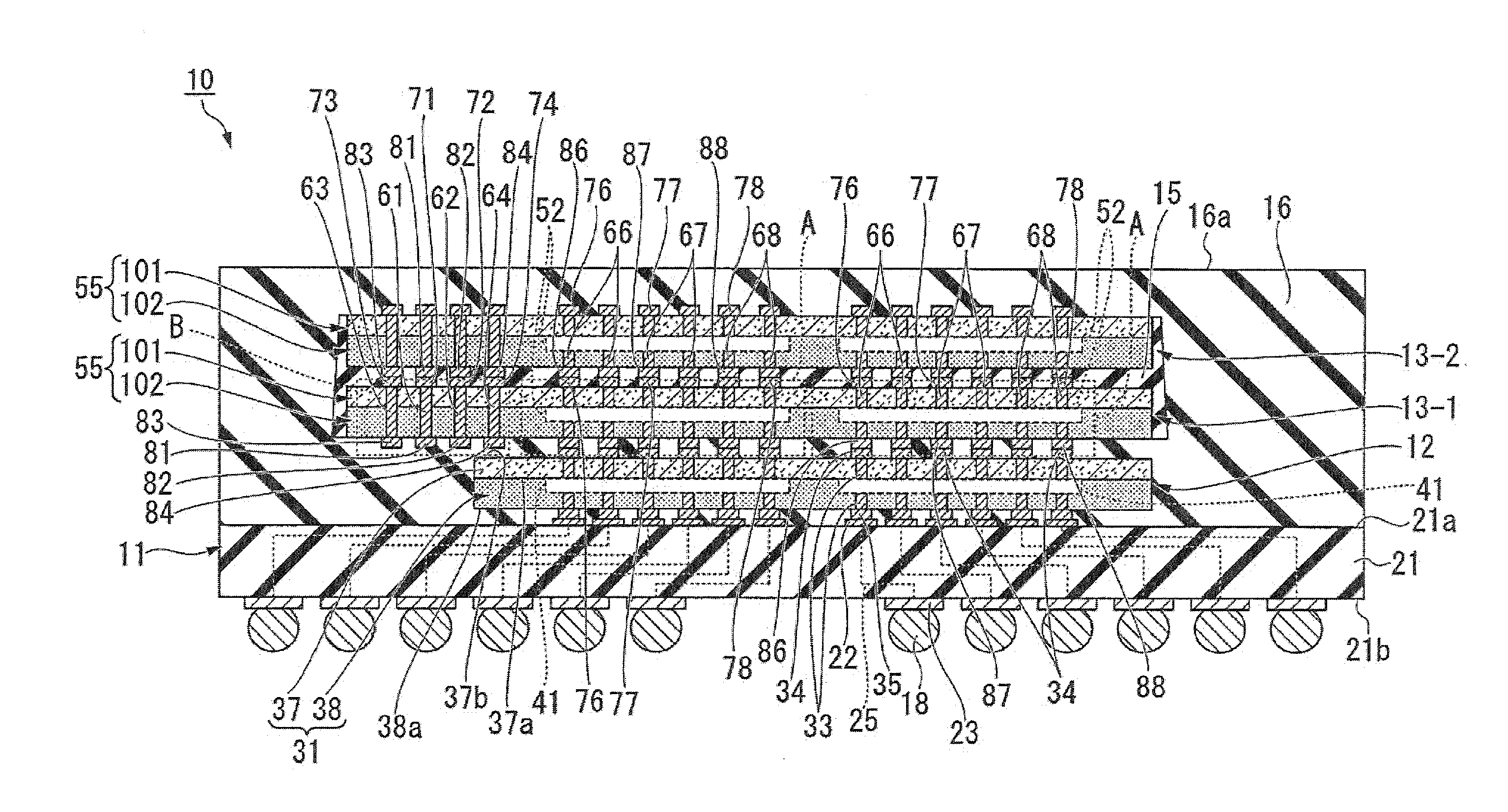
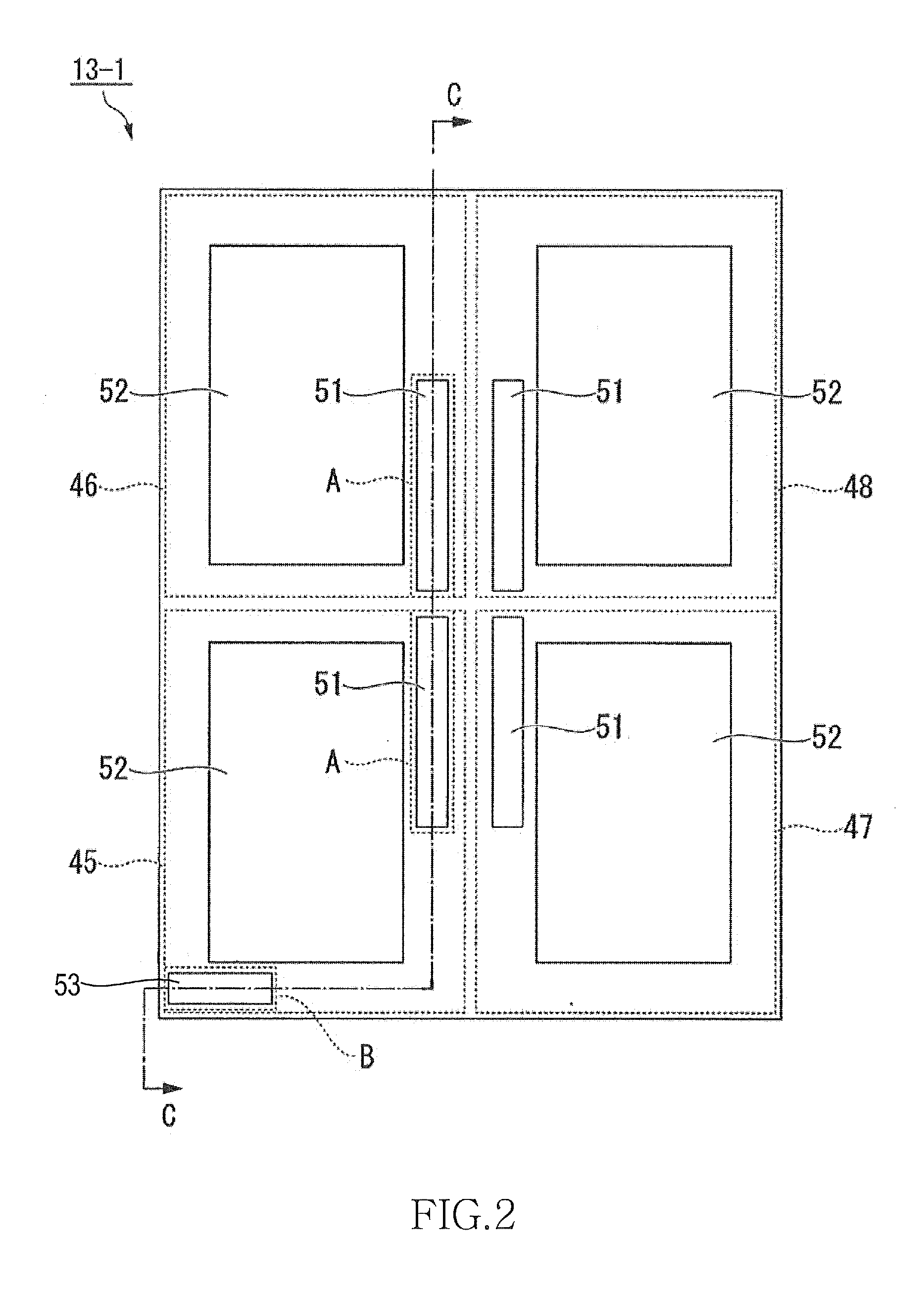
[0038]A stacked-type semiconductor device according to the first embodiment of the present invention will be explained with reference to FIGS. 1 and 2. A cross-sectional surface of a semiconductor chip 13-1 shown in FIG. 1 corresponds to a cross section of the semiconductor chip 13-1 taken along a C-C line of FIG. 2 described below.

[0039]An area A of FIG. 1 corresponds to the area A of FIG. 2, and an area B of FIG. 1 corresponds to the area B of FIG. 2.

[0040]As shown in FIG. 1, a stacked-type semiconductor device 10 according to the first embodiment has a wiring substrate (package substrate), a control semiconductor chip 12, semiconductor chips 13-1 and 13-2, a first encapsulating resin 15, a second encapsulating resin 16, and a plurality of external connection terminals 18.

[0041]The wiring substrate 11 has a substrate body 21, a plurality of connection pads 22, a plurality of external connection pads 23, and a plurality of wiring patterns 25. The substrate body 21 has a plate-like ...

second embodiment

[0186]Turning to FIG. 7, the same reference numerals are given to the same constituent elements as those of the semiconductor chip 13-1 illustrated in FIG. 3. In FIG. 7, the wide-IO DRAM which is a memory semiconductor chip is exemplified as a semiconductor chip 145 of the second embodiment.

[0187]Referring to FIG. 7, the semiconductor chip according to the second embodiment has the same configuration as that of the semiconductor chip 13-1 except that a first insulating ring 146, a second conductive path 147, a second insulating ring 151, and a third conductive path 152 are provided in place of the insulating ring 92 surrounding the through substrate conductor 111 of each of the first to fourth penetrating electrodes 61 to 64, the second conductive path 97 (a part of the seed layer 113 disposed from the inner surface of the through hole 103A in which the through substrate conductor 111 of the first penetrating electrode 61 is disposed to the inner surface of the through hole 103C in ...

third embodiment

[0221]Turning to FIG. 11, the same reference numerals are given to the same constituent elements as those of the structure illustrated in FIG. 1.

[0222]Referring to FIG. 11, a semiconductor chip 160 of the third embodiment has an internal circuit 162 including circuit elements, a power supply penetrating electrode group 163 including the plurality of power supply penetrating electrodes 66, a ground penetrating electrode group 164 including the plurality of ground penetrating electrodes 67, and signal penetrating electrode groups 165 to 168 each including the plurality of signal penetrating electrodes 68.

[0223]The internal circuit 162 has a function circuit unit 171 and an internal power supply generation circuit unit 172. The function circuit unit 171 has first to fourth channels 174 to 177.

[0224]The first channel 174 is electrically connected to the plurality of signal penetrating electrodes 68 constituting the signal penetrating electrode group 165. The first channel 174 exchanges ...


PUM


Abstract

Disclosed herein is a semiconductor chip that includes: a semiconductor chip body including a semiconductor substrate and a circuit element layer provided on a main surface of the semiconductor substrate, the circuit element layer including a plurality of circuit elements; first to fourth penetrating electrodes penetrating the semiconductor chip body; a first conductive path electrically connected between the first penetrating electrode and the second penetrating electrode without being in contact with any one of the circuit elements; a second conductive path electrically connected between the first penetrating electrode and the third penetrating electrode without being in contact with any one of the circuit elements; and a third conductive path electrically connected between the second penetrating electrode and the fourth penetrating electrode without being in contact with any one of the circuit elements.

Description

BACKGROUND OF THE INVENTION[0001]1. Field of the Invention[0002]The present invention relates to a semiconductor chip having plural penetrating electrodes that penetrate therethrough, a method of measuring a resistance thereof.[0003]2. Description of Related Art[0004]Along with miniaturization of electronic devices, demands for higher integration degree and miniaturization of semiconductor devices to be mounted in the electronic devices have arisen. Under such circumstances, a system-in-package technology in which various mounting structures are proposed is now attracting attention. In this technology, a plurality of semiconductor chips each having a circuit element layer are mounted in high density to achieve a sophisticated system in a short period.[0005]For example, a stacked-type semiconductor device in which a plurality of semiconductor chips are stacked in a three-dimensional manner is developed to achieve a miniaturization of the semiconductor device. In such a stacked-type s...

Claims


Application Information

Patent Timeline
Patent Type & Authority Applications(United States)
IPC IPC(8): H01L23/48
CPCH01L23/481H01L22/32H01L2224/16H01L22/34H01L22/14
Inventor TAKAKURA, KAZUYAISHIKAWA, TORU
Owner PS4 LUXCO SARL
Features
  • R&D
  • Intellectual Property
  • Life Sciences
  • Materials
  • Tech Scout
  • Unparalleled Data Quality
  • Higher Quality Content
  • 60% Fewer Hallucinations
Learn More