Supercharge Your Innovation With Domain-Expert AI Agents!

Dual work function finfet structures and methods for fabricating the same

a technology of finfets and work functions, which is applied in the direction of semiconductor devices, electrical equipment, basic electric elements, etc., can solve the problems of unacceptably high contact resistance of sram transistors in 3-d technology with intentional topography, further difficult control of silicide formation in 3-d technology, and the need for extra space for merging fins, etc., to achieve the effect of enhancing compressive stress

Inactive Publication Date: 2014-02-06
GLOBALFOUNDRIES US INC
View PDF1 Cites 17 Cited by
  • Summary
  • Abstract
  • Description
  • Claims
  • Application Information

AI Technical Summary

Benefits of technology

The present invention provides methods for fabricating FinFET structures with dual-workfunction capabilities. The methods involve depositing different materials in specific layers and etching them to create the desired structure. The resulting structure allows for more precise control over the threshold voltage of the FinFET, which can enhance performance and reliability. The technical effects include improved performance and reliability of the FinFET structure.

Problems solved by technology

It is further difficult to control silicide formation in a 3-D technology with intentional topography, aggravated by the presence of multiple crystal planes as well as non-uniform spacer profile across the gate-source / drain interface.
The SRAM transistor in such a device using currently known methods, however, would have unacceptably high contact resistance if a conventional silicide were formed.
However, merging the fins requires extra space in the SRAM to separate the n-type metal oxide semiconductor (NMOS) from the p-type metal oxide semiconductor (PMOS).
This severely increases the silicon area to manufacture a chip.
Also, contacting only from the top in 2-D rather than wrapping the contact around in 3-D severely decreases the contact area, thus increasing the contact-active resistance substantially and reducing device performance.

Method used


Image

  • Dual work function finfet structures and methods for fabricating the same
  • Dual work function finfet structures and methods for fabricating the same
  • Dual work function finfet structures and methods for fabricating the same

Examples


Embodiment Construction

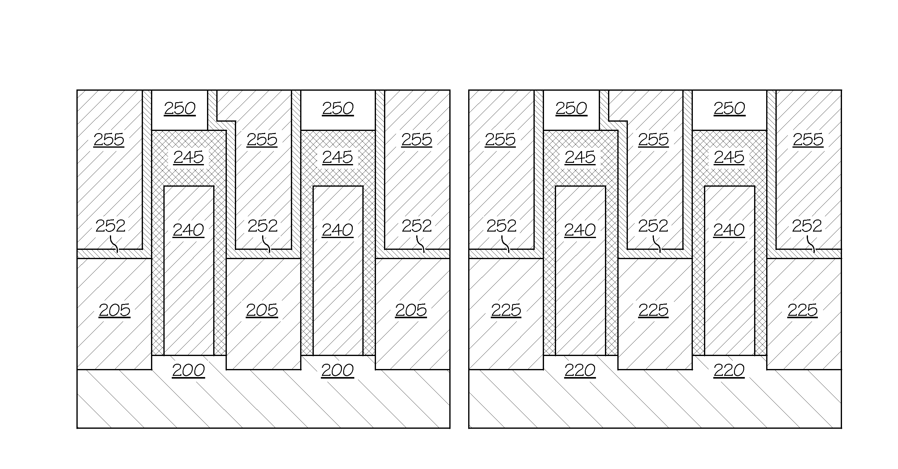
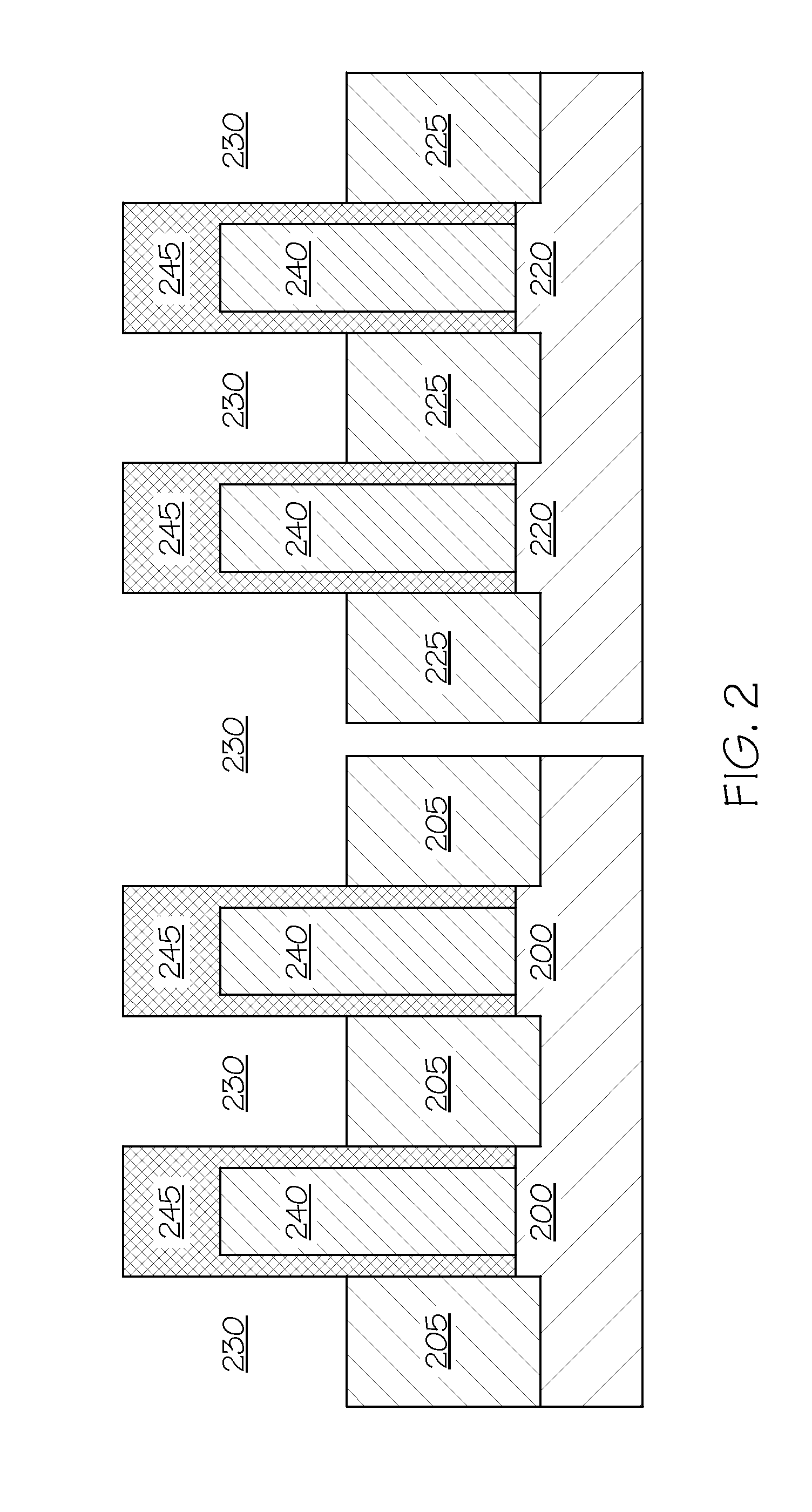
[0014]The following detailed description is merely exemplary in nature and is not intended to limit the invention or the application and uses of the invention. As used herein, the word “exemplary” means “serving as an example, instance, or illustration.” Thus, any embodiment described herein as “exemplary” is not necessarily to be construed as preferred or advantageous over other embodiments. All of the embodiments described herein are exemplary embodiments provided to enable persons skilled in the art to make or use the invention and not to limit the scope of the invention which is defined by the claims. Furthermore, there is no intention to be bound by any expressed or implied theory presented in the preceding technical field, background, brief summary, or the following detailed description.

[0015]For the sake of brevity, conventional techniques related to FinFET semiconductor device fabrication may not be described in detail herein. Moreover, the various tasks and process steps de...


PUM


Abstract

A method for fabricating a dual-workfunction FinFET structure includes depositing a first workfunction material in a layer in a plurality of trenches of the FinFET structure, depositing a low-resistance material layer over the first workfunction material layer, and etching the low-resistance material layer and the first workfunction material layer from a portion of the FinFET structure. The method further includes depositing a second workfunction material in a layer in a plurality of trenches of the portion and depositing a stress material layer over the second workfunction material layer.

Description

TECHNICAL FIELD[0001]The present invention generally relates to semiconductor devices and methods for fabricating semiconductor devices, and more particularly relates to FinFET structures having a dual workfunction and methods for fabricating the same.BACKGROUND[0002]In contrast to traditional planar metal-oxide-semiconductor field-effect transistors (MOSFETs), which are fabricated using conventional lithographic fabrication methods, non-planar FETs incorporate various vertical transistor structures. One such semiconductor structure is the “FinFET,” which takes its name from the multiple thin silicon “fins” that are used to form the respective gate channels, and which are typically on the order of tens of nanometers in width.[0003]More particularly, referring to the exemplary prior art nonplanar FET structure shown in FIG. 1, a FinFET 100 generally includes two or more parallel silicon fin structures (or simply “fins”) 104 and 106. These structures are typically formed using a silic...

Claims


Application Information

Patent Timeline
Patent Type & Authority Applications(United States)
IPC IPC(8): H01L21/336H01L21/311
CPCH01L21/823821H01L29/7843H10B10/00
Inventor WEI, ANDY C.YANG, BINTAMBWE, FRANCIS M.
Owner GLOBALFOUNDRIES US INC
Features
  • R&D
  • Intellectual Property
  • Life Sciences
  • Materials
  • Tech Scout
  • Unparalleled Data Quality
  • Higher Quality Content
  • 60% Fewer Hallucinations
Learn More