Graphene-based terahertz devices
- Summary
- Abstract
- Description
- Claims
- Application Information
AI Technical Summary
Benefits of technology
Problems solved by technology
Method used
Image
Examples
Embodiment Construction
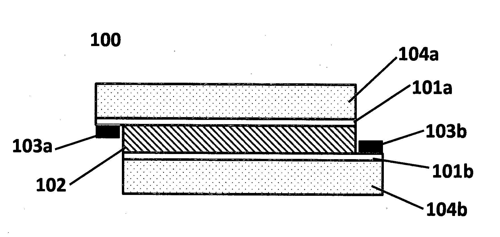
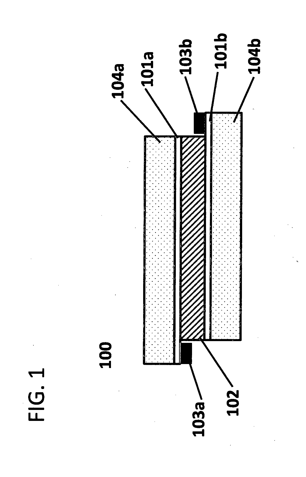
[0019]FIG. 1 is a diagram that shows schematically a graphene-based THz device 100 of the this invention. The graphene-based THz device 100 includes a top graphene layer 101a, a bottom graphene layer 101b, and a middle layer 102 sandwiched between the top graphene layer 101a and the bottom graphene layer 101b. The middle layer 102 is a liquid crystal layer, a piezocrystal layer, an ionic liquid layer, or an ion gel layer. The top graphene layer 101a and the bottom graphene layer 101b each have an electrode deposited on one of its edge, i.e., a first electrode 103a and a second electrode 103b. The first electrode 103a and the second electrode 103b are vertically misaligned to prevent short circuit through the middle layer 102. Also included in the graphene-based THz device 100 are two layers of dielectric material 104a and 104b, covering the top surface of graphene layer 101a and the bottom surface of the bottom graphene layer 101b, respectively.
[0020]The graphene-based THz device 10...
PUM
 Abstract
Description
Claims
Application Information
 - R&D
- Intellectual Property
- Life Sciences
- Materials
- Tech Scout
- Unparalleled Data Quality
- Higher Quality Content
- 60% Fewer Hallucinations
Browse by: Latest US Patents, China's latest patents, Technical Efficacy Thesaurus, Application Domain, Technology Topic, Popular Technical Reports.
© 2025 PatSnap. All rights reserved.Legal|Privacy policy|Modern Slavery Act Transparency Statement|Sitemap|About US| Contact US: help@patsnap.com


