Switch circuit
- Summary
- Abstract
- Description
- Claims
- Application Information
AI Technical Summary
Benefits of technology
Problems solved by technology
Method used
Image

Examples
first embodiment
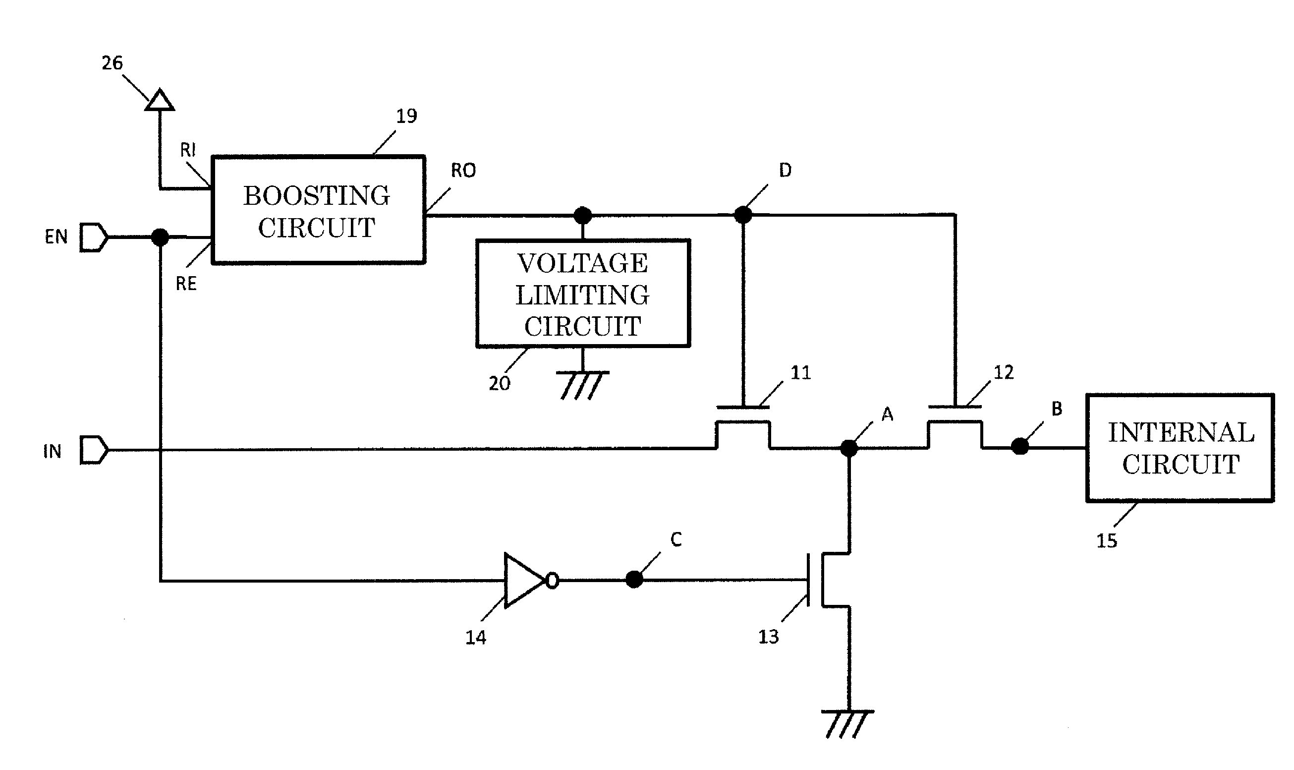
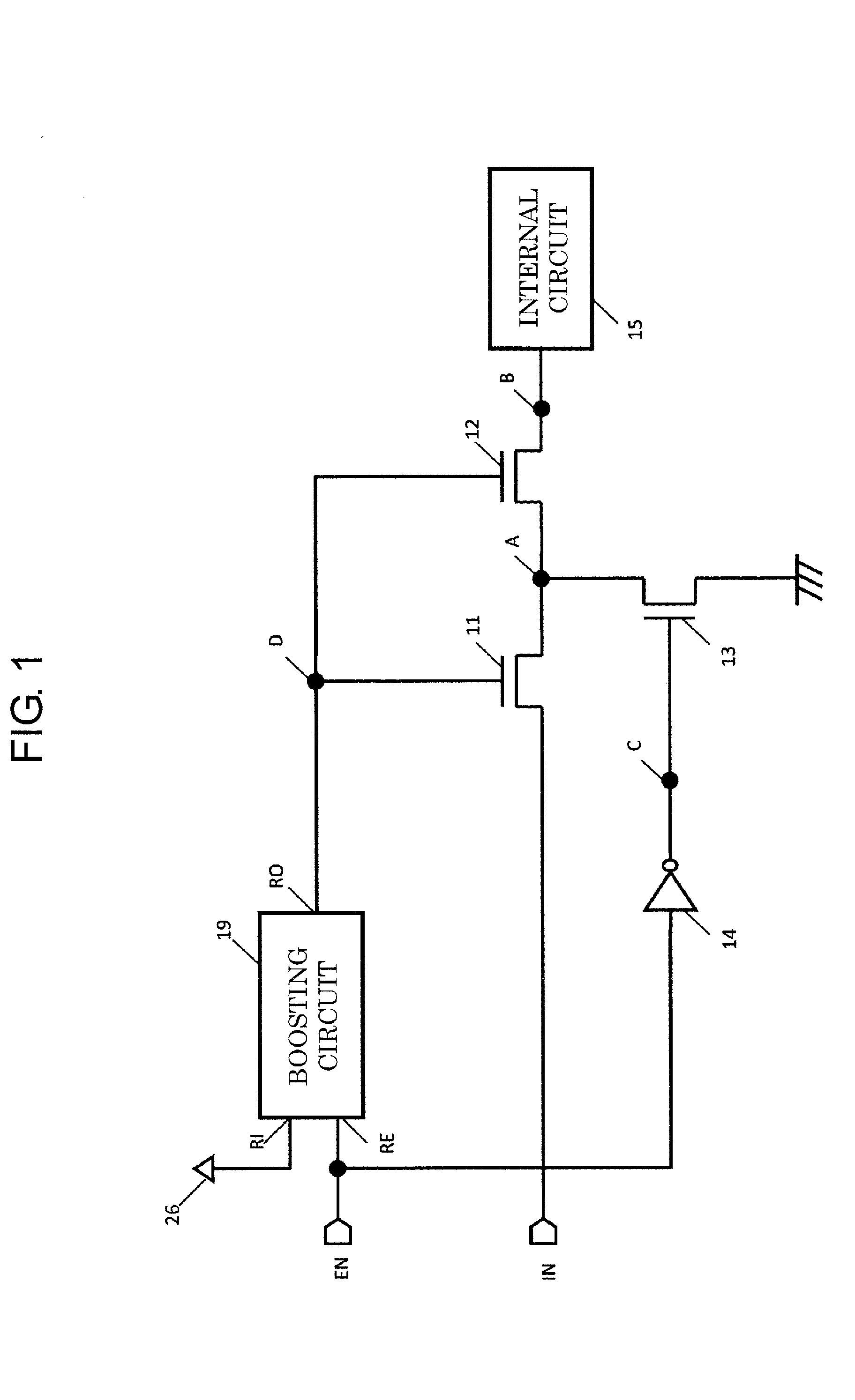
[0022]FIG. 1 is a circuit diagram illustrating a switch circuit according to a first embodiment.
[0023]The switch circuit according to the first embodiment is equipped with NMOS transistors 11, 12 and 13, an inverter 14, and a boosting circuit 19.
[0024]The NMOS transistor 11 has a drain connected to the input terminal IN, a gate connected to a voltage output terminal RO (node D) of the boosting circuit 19, and a source connected to a drain of the NMOS transistor 12 and a drain of the NMOS transistor 13. The NMOS transistor 12 has a gate connected to the voltage output terminal RO (node D) of the boosting circuit 19, and a source connected to an input terminal (node B) of the internal circuit 15. The NMOS transistor 13 has the drain connected to the source of the NMOS transistor 11 and the drain of the NMOS transistor 12, a gate connected to an output terminal (node C) of the inverter 14, and a source grounded to GND. The inverter 14 has an input terminal connected to the switch contr...
second embodiment
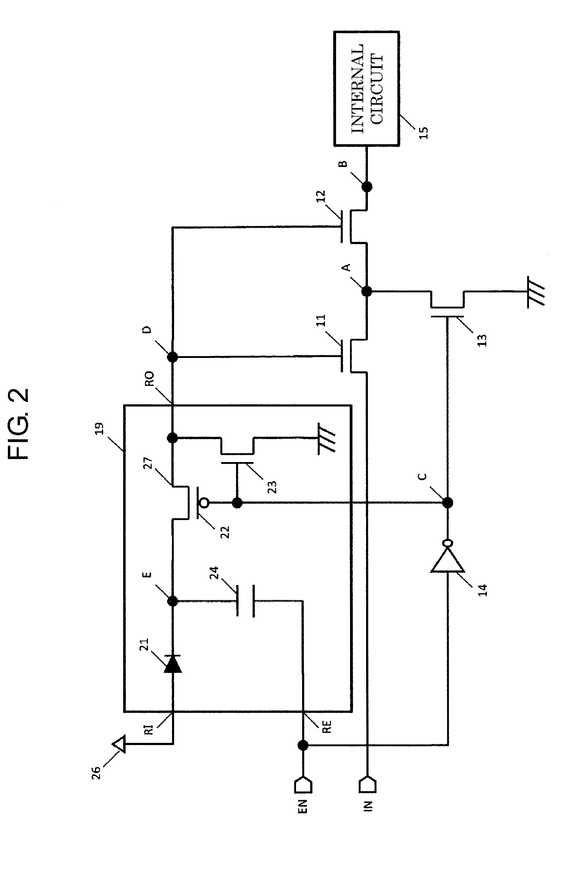
[0042]FIG. 3 is a circuit diagram illustrating a switch circuit according to a second embodiment.
[0043]The switch circuit according to the second embodiment is equipped with a voltage limiting circuit 20 in addition to the switch circuit according to the first embodiment. The voltage limiting circuit 20 has one end connected to the voltage output terminal RO (node D) of the boosting circuit 19, and the other end connected to GND.
[0044]The voltage limiting circuit 20 allows current to flow into GND when the voltage output terminal RO of the boosting circuit 19 is at greater than equal to a voltage VBD2, to thereby maintain the voltage at less than or equal to VBD2. Here, VBD2 is a voltage greater than or equal to (VDD+VGSN1+VOVN1) and a voltage lower than the gate breakdown voltage of the NMOS transistors 11 and 12.
[0045]Thus, in the switch circuit according to the second embodiment, even when the output voltage of the boosting circuit 19 becomes the voltage greater than or equal to ...
PUM
 Abstract
Description
Claims
Application Information
 - Generate Ideas
- Intellectual Property
- Life Sciences
- Materials
- Tech Scout
- Unparalleled Data Quality
- Higher Quality Content
- 60% Fewer Hallucinations
Browse by: Latest US Patents, China's latest patents, Technical Efficacy Thesaurus, Application Domain, Technology Topic, Popular Technical Reports.
© 2025 PatSnap. All rights reserved.Legal|Privacy policy|Modern Slavery Act Transparency Statement|Sitemap|About US| Contact US: help@patsnap.com