Supercharge Your Innovation With Domain-Expert AI Agents!

Ohmic contact of thin film solar cell

a solar cell and thin film technology, applied in the field of contact structures, can solve the problems of reducing the efficiency of the solar cell, degrading the electrical contact between the absorber poor ohmic contact between the molybdenum layer and the absorber layer, so as to reduce the chalcogenization of the transition metal, reduce the contact resistance, and reduce the effect of contact resistan

Active Publication Date: 2016-12-29
INT BUSINESS MASCH CORP
View PDF9 Cites 0 Cited by
  • Summary
  • Abstract
  • Description
  • Claims
  • Application Information

AI Technical Summary

Benefits of technology

The solution effectively reduces contact resistance and enhances the efficiency of solar cells by maintaining reliable electrical contact even with gaps or variations in the chalcogenide formation process, improving the overall performance of the solar cell.

Problems solved by technology

Formation of excess molybdenum disulfide between a molybdenum layer and the absorber layer may cause a poor ohmic contact between the molybdenum layer and the absorber layer.
Further, due to high compressive stress developed in the absorber layer, gaps can be formed within the molybdenum sulfide layer, and significantly degrade the electrical contact between the absorber layer and the molybdenum layer.
By effectively reducing the total contact area between the absorber layer and the molybdenum layer, such gaps increase the series resistance of a solar cell, and reduces the efficiency of the solar cell.

Method used


Image

  • Ohmic contact of thin film solar cell
  • Ohmic contact of thin film solar cell
  • Ohmic contact of thin film solar cell

Examples


Embodiment Construction

[0015]As stated above, the present disclosure relates to low resistance contact structures between a transition metal layer and a semiconductor chalcogenide material, and methods of manufacturing the same, which are now described in detail with accompanying figures. It is noted that like reference numerals refer to like elements across different embodiments.

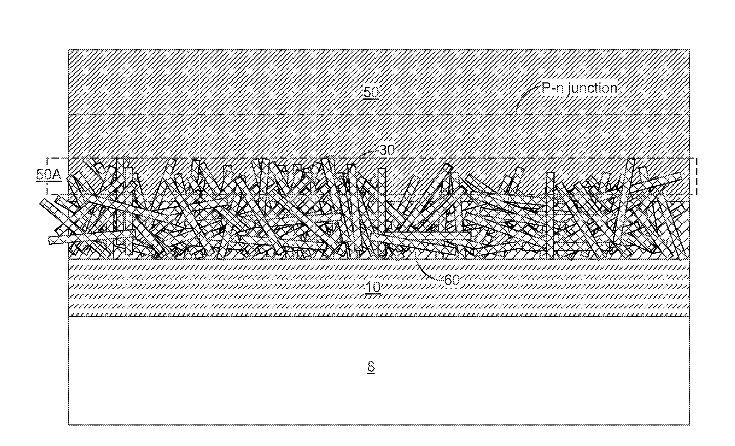
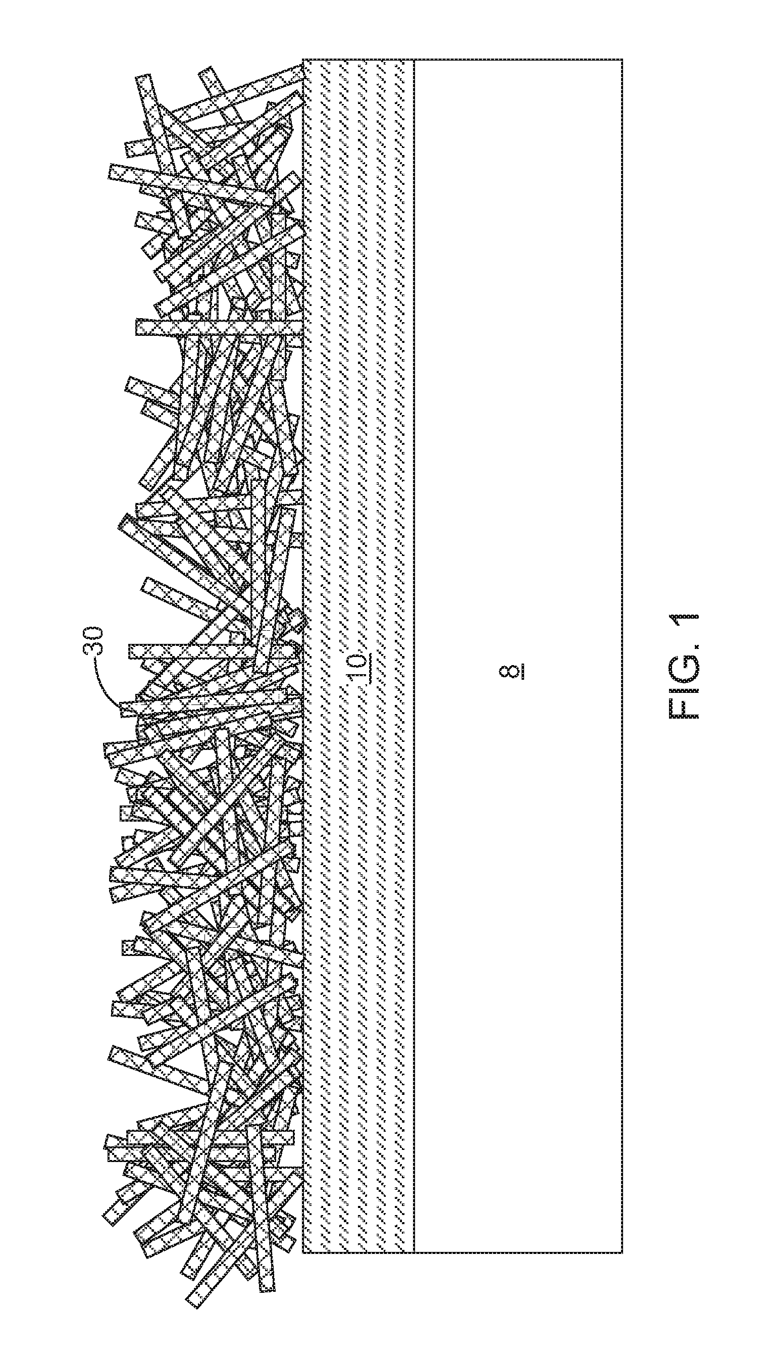
[0016]Referring to FIG. 1, a first exemplary structure according to a first embodiment of the present disclosure includes a transition metal layer 10 formed on a substrate 8. In one embodiment, the substrate 8 can be an insulator substrate including a dielectric material such as glass or a plastic material. In another embodiment, the substrate 8 can be a metallic substrate including a diffusion barrier layer on the top surface thereof. The diffusion barrier layer can be a metallic nitride layer such as tantalum nitride or titanium nitride, and prevents diffusion of metallic materials from a lower portion of the substrate 8 to a t...


PUM

PropertyMeasurementUnit
work functionaaaaaaaaaa
work functionsaaaaaaaaaa
thicknessesaaaaaaaaaa

Abstract

A chalcogen-resistant material including at least one of a conductive elongated nanostructure layer and a high work function material layer is deposited on a transition metal layer on a substrate. A semiconductor chalcogenide material layer is deposited over the chalcogen-resistant material. The conductive elongated nanostructures, if present, can reduce contact resistance by providing direct electrically conductive paths from the transition metal layer through the chalcogen-resistant material and to the semiconductor chalcogenide material. The high work function material layer, if present, can reduce contact resistance by blocking chalcogenization of the transition metal in the transition metal layer. Reduction of the contact resistance can enhance efficiency of a solar cell including the chalcogenide semiconductor material.

Description

BACKGROUND[0001]The present disclosure relates to contact structures, and particularly to low resistance contact structures between a transition metal layer and a semiconductor material, and methods of manufacturing the same.[0002]Many thin film solar cells include a chalcogenide in an absorber layer. The chalcogenide can be a chalcopyrite such as CuIn(S,Se)2(CIS) and CuInGaSe2 (CIGS), kesterite (Cu2(Zn, Fe) Sn (Se,S)4, Ga(S,Se), GaTe, In2(S,Se)3, and InTe, CdTe, Cd(S, Se), ZnTe, Pb(Se,S), Zn(S, Se), W(S,Se)2, Bi2S3, Ag2S, NiS, ZnO, Cu2O, CuO, Cu2S, FeS2. These solar cells have been fabricated using different process like PVD, CVD, solution processes, or electrochemical deposition process.[0003]For example, in thin films solar cells, a back contact material such as molybdenum is deposited on a dielectric substrate. Absorber layers, such as a stack of a p-type semiconductor material and an n-type semiconductor material, are deposited on the back contact material. Whether sulfur, sele...

Claims


Application Information

Patent Timeline
Patent Type & Authority Applications(United States)
IPC IPC(8): H01L31/0224H01L31/032
CPCH01L31/022441H01L31/0322B82Y30/00H01L31/032H01L31/0326H01L31/022425H01L31/03923H01L31/0749Y02E10/541
Inventor AHMED, SHAFAATDELIGIANNI, HARIKLIAROMANKIW, LUBOMYR T.
Owner INT BUSINESS MASCH CORP
Features
  • R&D
  • Intellectual Property
  • Life Sciences
  • Materials
  • Tech Scout
  • Unparalleled Data Quality
  • Higher Quality Content
  • 60% Fewer Hallucinations
Learn More