Supercharge Your Innovation With Domain-Expert AI Agents!

Co-integration of tensile silicon and compressive silicon germanium

a technology of compressive silicon and germanium, which is applied in the direction of basic electric elements, electrical equipment, and semiconductor devices, can solve the problems of internal strain, affecting the crystal lattice, and creating strain by incorporating germanium atoms using existing methods

Active Publication Date: 2017-07-13
STMICROELECTRONICS INC
View PDF0 Cites 4 Cited by
  • Summary
  • Abstract
  • Description
  • Claims
  • Application Information

AI Technical Summary

Benefits of technology

This approach allows for independently adjustable strain properties in pFETs and nFETs, enhancing electron and hole mobility while reducing defects, thereby improving the aspect ratio and performance of FinFETs.

Problems solved by technology

The presence of germanium atoms having longer bonds stretches the lattice, causing internal strain.
While a strained silicon lattice is beneficial, creating strain by incorporating germanium atoms using existing methods tends to damage the crystal lattice.
As a result, the lattice structures of germanium-rich films tend to be mechanically unstable, especially if they contain a high number of structural defects such as faults, or dislocations.
Furthermore, a mechanically unstable SiGe fin may be structurally limited with regard to its aspect ratio, or height-to-width ratio.
Such a limitation is undesirable because one advantage of a FinFET is that the fin, being a vertical structure, has a small footprint.

Method used


Image

  • Co-integration of tensile silicon and compressive silicon germanium
  • Co-integration of tensile silicon and compressive silicon germanium
  • Co-integration of tensile silicon and compressive silicon germanium

Examples


Embodiment Construction

[0029]In the following description, certain specific details are set forth in order to provide a thorough understanding of various aspects of the disclosed subject matter. However, the disclosed subject matter may be practiced without these specific details. In some instances, well-known structures and methods of semiconductor processing have not been described in detail to avoid obscuring the descriptions of other aspects of the present disclosure.

[0030]Unless the context requires otherwise, throughout the specification and claims that follow, the word “comprise” and variations thereof, such as “comprises” and “comprising” are to be construed in an open, inclusive sense, that is, as “including, but not limited to.”

[0031]Reference throughout the specification to “one embodiment” or “an embodiment” means that a particular feature, structure, or characteristic described in connection with the embodiment is included in at least one embodiment. Thus, the appearance of the phrases “in on...


PUM


Abstract

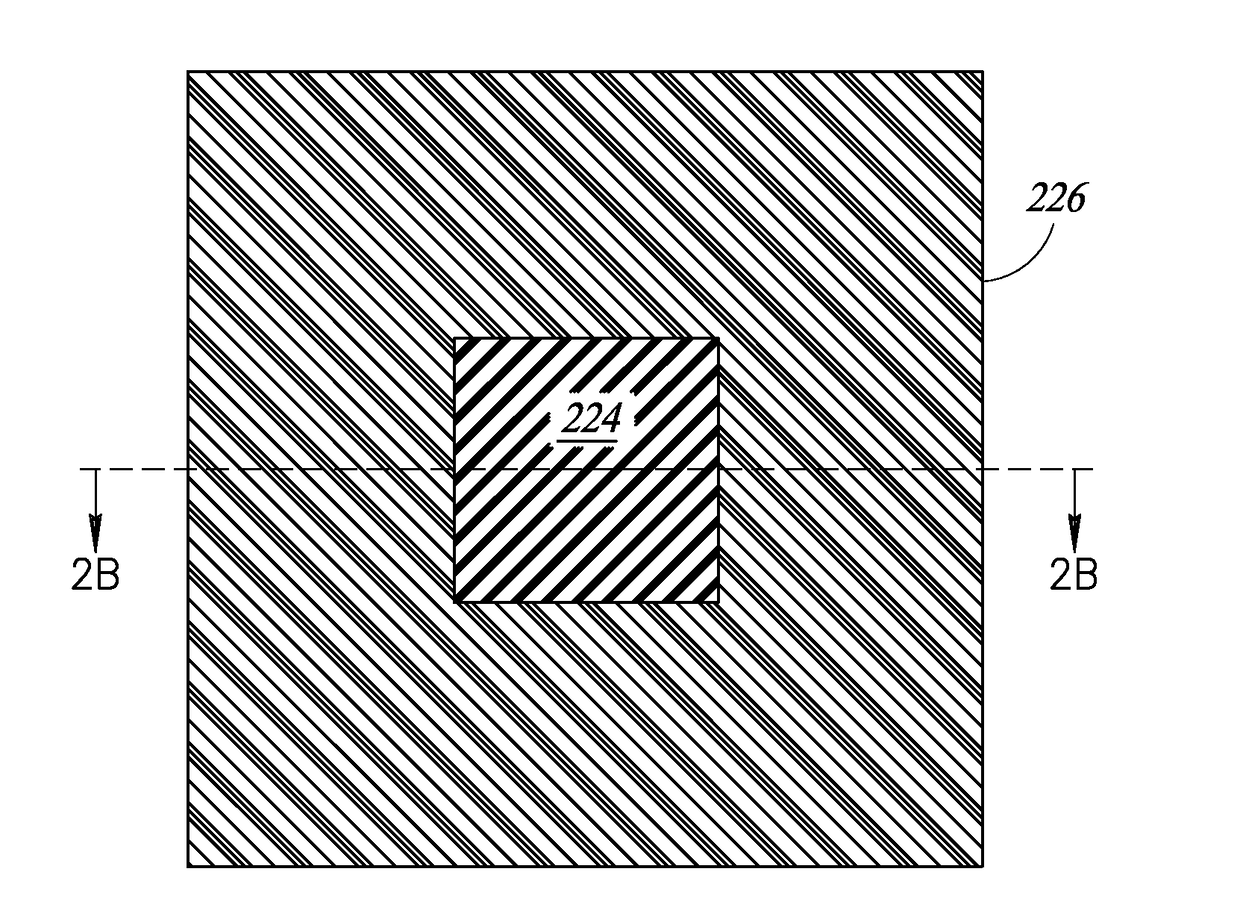
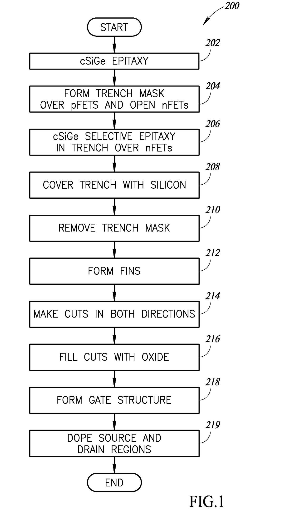
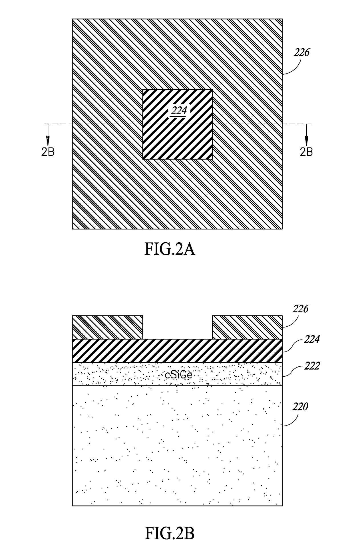
Integrated circuits are disclosed in which the strain properties of adjacent pFETs and nFETs are independently adjustable. The pFETs include compressive-strained SiGe on a silicon substrate, while the nFETs include tensile-strained silicon on a strain-relaxed SiGe substrate. Adjacent n-type and p-type FinFETs are separated by electrically insulating regions formed by a damascene process. During formation of the insulating regions, the SiGe substrate supporting the n-type devices is permitted to relax elastically, thereby limiting defect formation in the crystal lattice of the SiGe substrate.

Description

BACKGROUND[0001]Technical Field[0002]The present disclosure generally relates to techniques for fabricating high performance fin field-effect transistors (FinFETs) and, in particular, to techniques for defect reduction in strained silicon transistors.[0003]Description of the Related Art[0004]Advanced integrated circuits often feature strained channel transistors, silicon-on-insulator (SOI) substrates, FinFET structures, or combinations thereof, in order to continue scaling transistor gate lengths below 20 nm. Such technologies allow the channel length of the transistor to be made smaller while minimizing detrimental consequences such as current leakage and other short channel effects.[0005]A FinFET is an electronic switching device that features a conduction channel in the form of a semiconducting fin that extends outward from the substrate surface. In such a device, the gate, which controls current flow in the fin, wraps around three sides of the fin so as to influence current flow...

Claims


Application Information

Patent Timeline
Patent Type & Authority Applications(United States)
IPC IPC(8): H01L21/8238H01L29/417H01L29/78
CPCH01L21/823821H01L29/41791H01L29/785H01L27/0924H01L29/165H01L21/823807H01L21/823878H01L21/02381H01L21/02532H01L21/76224H01L27/0922H01L29/4916H01L29/7842H01L29/0649
Inventor LOUBET, NICOLASMORIN, PIERREMIGNOT, YANN
Owner STMICROELECTRONICS INC
Features
  • R&D
  • Intellectual Property
  • Life Sciences
  • Materials
  • Tech Scout
  • Unparalleled Data Quality
  • Higher Quality Content
  • 60% Fewer Hallucinations
Learn More