Organic light-emitting diode panel and manufacturing method using the same

Active Publication Date: 2018-04-19
FOCALTECH SYSTEMS LTD
View PDF0 Cites 0 Cited by
  • Summary
  • Abstract
  • Description
  • Claims
  • Application Information

AI Technical Summary

Benefits of technology

[0010]An objective of the present invention is to provide an organic light-emitting diode panel and a manufacturing method thereof t

Problems solved by technology

1. Because the organic materials are very thin, about 1000˜2000 Å in total, the circuits between the anode and cathode would be easily short circuit. It causes dot defect of the OLED display, unusual high current and the reduction of the production yield.
2. Because the low aperture ratio of the glass substrate of the thin film transistor, the bottom emission OLED has insufficient brightness.
3. The top emission OLED requires a high conduction and a high transparent material to serve as cathode. However, the ca

Method used


Image

  • Organic light-emitting diode panel and manufacturing method using the same
  • Organic light-emitting diode panel and manufacturing method using the same
  • Organic light-emitting diode panel and manufacturing method using the same

Examples


Example

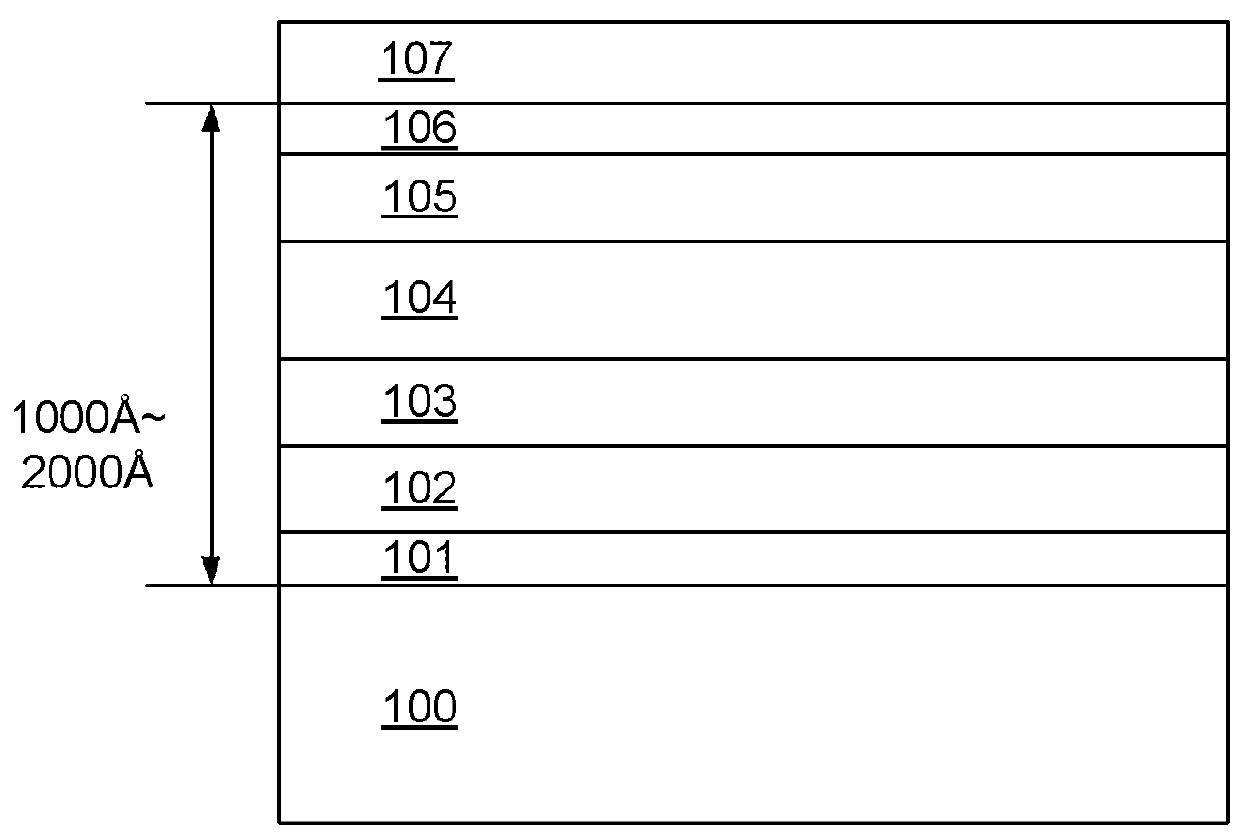
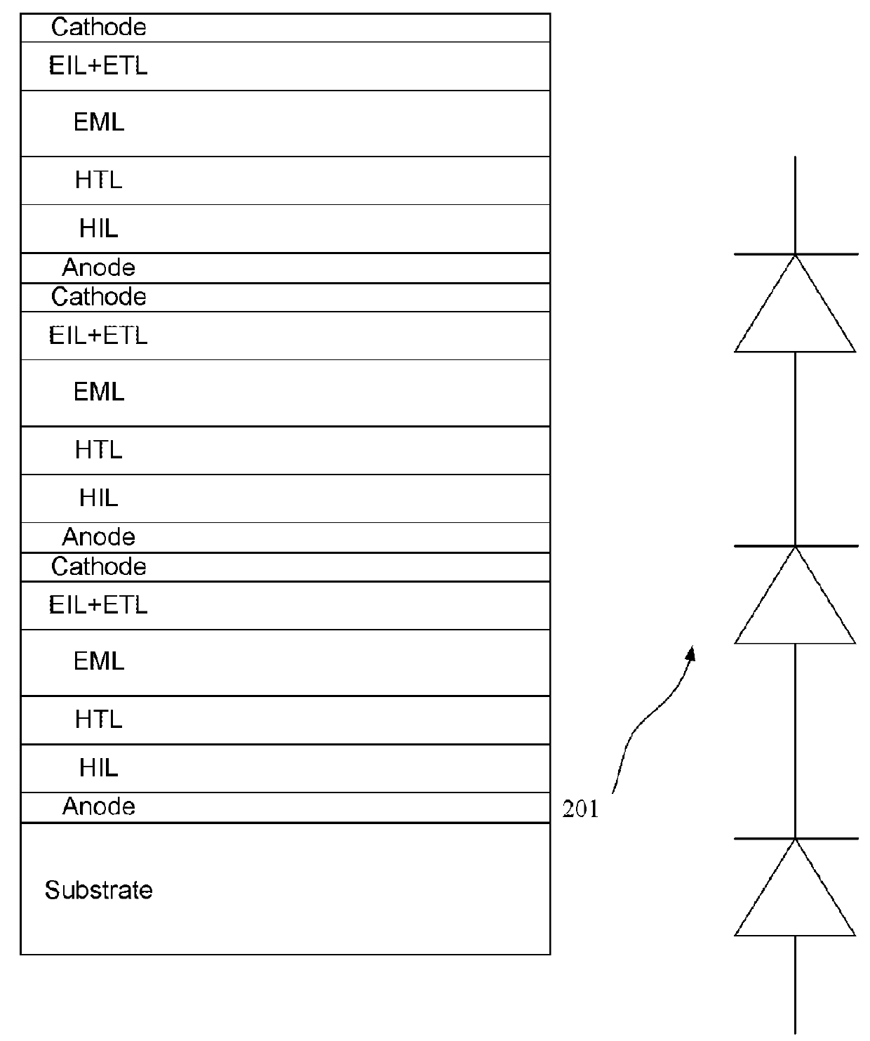
[0095]In the embodiments and claims, spatially relative terms, such as “underlying,”“below,”“lower,”“overlying,”“upper” and the like, may be used herein for ease of description to describe one element or feature's relationship to another element(s) or feature(s) as illustrated in the figures. Those skilled in the art may understand that the spatially relative terms are intended to encompass different orientations of the apparatus in use or operation in addition to the orientation depicted in the figures. For example, if an apparatus in the drawing is turned over, elements or features described as “below” or “beneath” other elements or features would then be oriented “above” the other elements. The terms “below” or “beneath” can, therefore, encompass both an orientation of above and below. If the apparatus may be otherwise oriented (rotated 90 degrees or at other orientations), then the spatially relative descriptors used herein may likewise be interpreted accordingly.
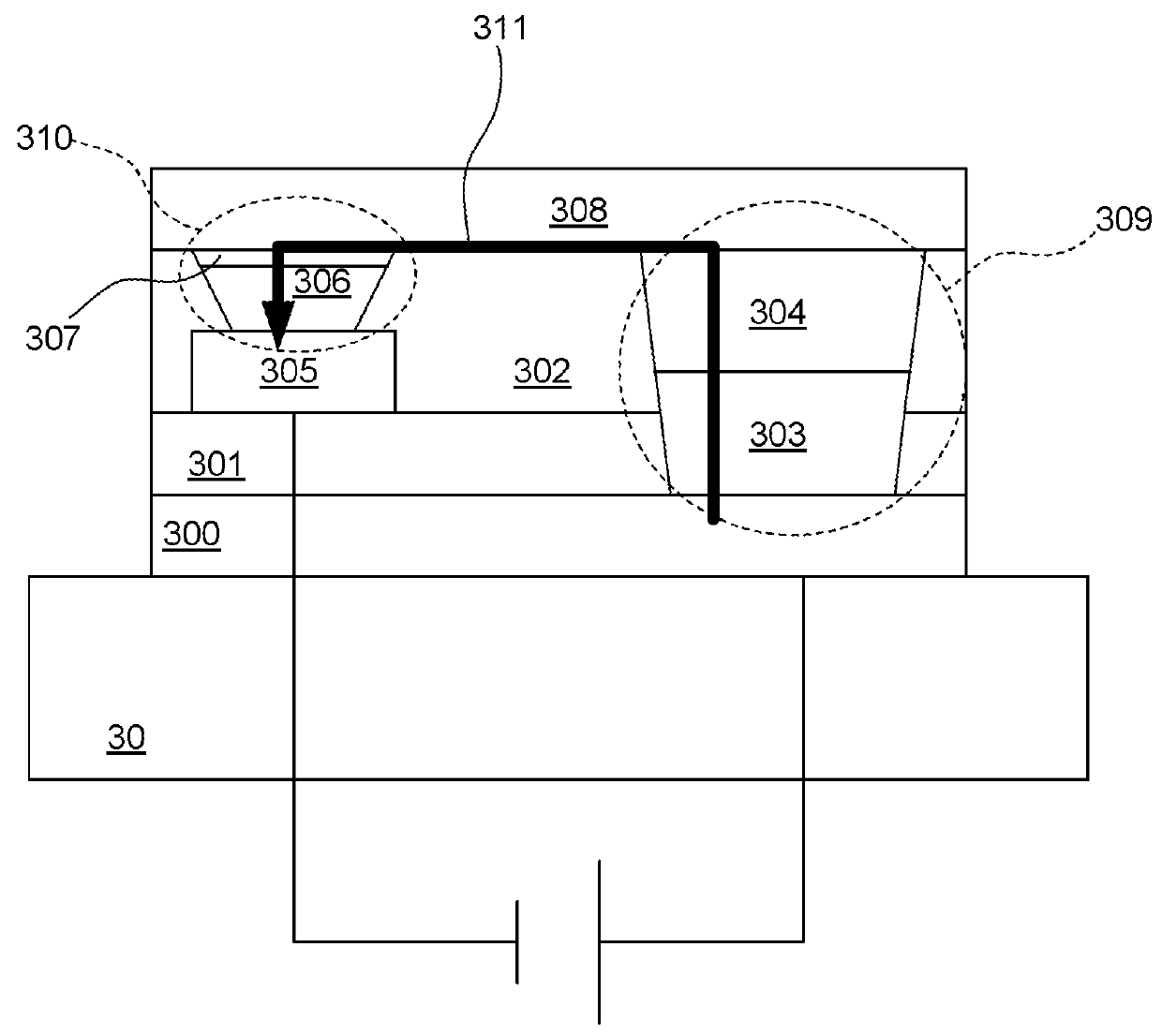
[0096]FIG. 3 il...


PUM


Abstract

An organic light-emitting diode panel and a manufacturing method using the same are provided in the present invention. The OLED panel includes at least a pixel. The pixel includes a anode conducting layer, an insulation layer, an emitting layer (EML), a cathode layer and a reference voltage layer. The anode conducting layer is disposed on a transparent substrate. The insulation layer is disposed on the anode conducting layer and has a first cavity and a second cavity, wherein there is a distance between the first anode layer and the bottom of second cavity. There are a hole injection layer (HIL) and a hole transmission layer (HTL). The HIL is disposed on the first anode conducting layer. The HTL is disposed on the HIL. There are a cathode layer, an electronic injection layer (EIL) and an electronic transmission layer (ETL) in the second cavity. The cathode layer is exposed by the bottom of the second cavity. The EIL is disposed on the cathode layer. The ETL is disposed on the EIL. The EML is disposed on the insulation layer. The reference voltage layer is disposed on the EML.

Description

BACKGROUND OF THE INVENTION[0001]This application claims priorities of No. 105133678 filed in Taiwan R.O.C. on Oct. 19, 2016 and No. 106121905 filed in Taiwan R.O.C. on Jun. 30, 2017 under 35 USC 119, the entire content of which is hereby incorporated by reference.FIELD OF THE INVENTION[0002]The present invention relates to the technology of an organic light-emitting diode, and more particularly, to an organic light-emitting diode panel and a manufacturing method thereof.DESCRIPTION OF THE RELATED ART[0003]The conventional organic light-emitting diode (OLED) device has a vertical stacked layer of the organic material layers by evaporating process as shown in FIG. 1. FIG. 1 illustrates a structure of the current OLED device. Referring to FIG. 1, the OLED device includes a glass substrate 100, an anode layer 101, a hole injection layer (HIL) 102, a hole transport layer (HTL) 103, an organic emitting layer (EML) 104, an electron transport layer (ETL) 105, an electron injection layer (E...

Claims


Application Information

Patent Timeline
IPC IPC(8): H01L27/32H01L51/52H01L51/50H01L51/05
CPCH01L27/3244H01L51/5206H01L51/5221H01L51/5056H01L51/0508H10K59/1213H10K59/12H10K50/13H10K50/125H10K50/80H10K50/16H10K50/15H10K50/82H10K50/30H10K50/11H10K2102/341H10K59/805H10K10/46H10K50/81H10K50/805
Inventor WANG, CHUN-FU
Owner FOCALTECH SYSTEMS LTD
Why Eureka
Try Eureka