Supercharge Your Innovation With Domain-Expert AI Agents!

Thermal Reflector Device for Semiconductor Fabrication Tool

a technology of reflector device and semiconductor, which is applied in the direction of coating, chemical vapor deposition coating, metallic material coating process, etc., can solve the problems of critical defects, increase in design and manufacturing complexity, and inability to meet the needs of the next generation of integrated circuits

Active Publication Date: 2018-12-13
TAIWAN SEMICON MFG CO LTD
View PDF9 Cites 0 Cited by
  • Summary
  • Abstract
  • Description
  • Claims
  • Application Information

AI Technical Summary

Benefits of technology

This approach results in more uniform substrate heating, reducing temperature variability and enhancing the yield of epitaxial material deposition, addressing the limitations of conventional systems by controlling where thermal energy falls on the substrate.

Problems solved by technology

However, such scaling down has also been accompanied by increased complexity in design and manufacturing of devices incorporating these ICs, and, for these advances to be realized, similar developments in device design are needed.
Epitaxy is capable of producing layers of highly uniform thickness; however minute deviations that may be perfectly acceptable in one technology may be critical defects once the design node shrinks.
Accordingly, while conventional systems and techniques of epitaxial deposition have been adequate for previous designs, they may not be able to meet the needs of the next generation of integrated circuits.

Method used


Image

  • Thermal Reflector Device for Semiconductor Fabrication Tool
  • Thermal Reflector Device for Semiconductor Fabrication Tool
  • Thermal Reflector Device for Semiconductor Fabrication Tool

Examples


Embodiment Construction

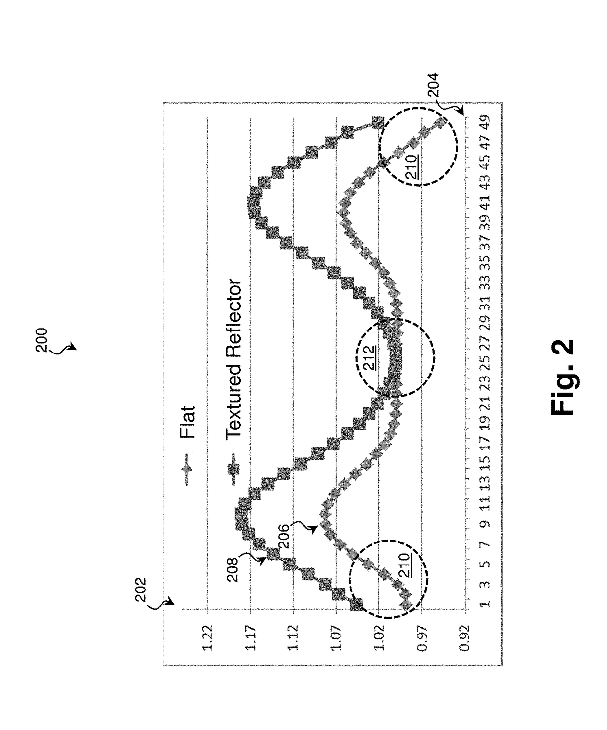
[0017]The present disclosure relates generally to IC device manufacturing and, more particularly, to a system for thermal treatment of a substrate with improved thermal uniformity.

[0018]The following disclosure provides many different embodiments, or examples, for implementing different features of the disclosure. Specific examples of components and arrangements are described below to simplify the present disclosure. These are, of course, merely examples and are not intended to be limiting. For example, the formation of a first feature over or on a second feature in the description that follows may include embodiments in which the first and second features are formed in direct contact, and may also include embodiments in which additional features may be formed between the first and second features, such that the first and second features may not be in direct contact. In addition, the present disclosure may repeat reference numerals and / or letters in the various examples. This repeti...


PUM

PropertyMeasurementUnit
peak-to-trough heightaaaaaaaaaa
temperatureaaaaaaaaaa

Abstract

A system and apparatus for thermal treatment of a substrate with improved thermal uniformity is provided. In some embodiments, the system includes a heating element, a substrate-retaining element operable to retain a substrate, and a reflective structure operable to direct thermal energy of the heating element towards the substrate retained in the substrate-retaining element. The reflective structure includes a textured portion wherein a texture of the textured portion is configured to direct the thermal energy towards the retained substrate. In some such embodiments, the texture includes a roughened irregular surface configured to direct the thermal energy towards the retained substrate. In some such embodiments, the texture includes a plurality of circumferential ridge structures configured to direct the thermal energy towards the retained substrate.

Description

PRIORITY DATA[0001]This application is a Divisional of U.S. patent application Ser. No. 15 / 287,434, filed Oct. 6, 2016, which further claims the benefit of U.S. Prov. App. No. 62 / 288,663 entitled “Thermal Reflector Device for Semiconductor Fabrication Tools,” filed Jan. 29, 2016, herein incorporated by reference in its entirety.BACKGROUND[0002]The semiconductor integrated circuit (IC) industry has experienced rapid growth. In the course of IC evolution, functional density (i.e., the number of interconnected devices per chip area) has generally increased while geometry size (i.e., the smallest component (or line) that can be created using a fabrication process) has decreased. This scaling down process generally provides benefits by increasing production efficiency and lowering associated costs. However, such scaling down has also been accompanied by increased complexity in design and manufacturing of devices incorporating these ICs, and, for these advances to be realized, similar dev...

Claims


Application Information

Patent Timeline
Patent Type & Authority Applications(United States)
IPC IPC(8): H01L21/67C23C16/46C23C16/48
CPCH01L21/67115C23C16/46C23C16/481H01L21/67098
Inventor HUNG, SHIH-WEI
Owner TAIWAN SEMICON MFG CO LTD
Features
  • R&D
  • Intellectual Property
  • Life Sciences
  • Materials
  • Tech Scout
  • Unparalleled Data Quality
  • Higher Quality Content
  • 60% Fewer Hallucinations
Learn More