Semiconductor substrate and method for manufacturing the same
a semiconductor substrate and semiconductor technology, applied in the field of semiconductor substrates, can solve problems such as serious bridge problems in semiconductor substrates with fine pitch, and achieve the effect of reducing bridge and short circuit formation
- Summary
- Abstract
- Description
- Claims
- Application Information
AI Technical Summary
Benefits of technology
Problems solved by technology
Method used
Image

Examples
Embodiment Construction
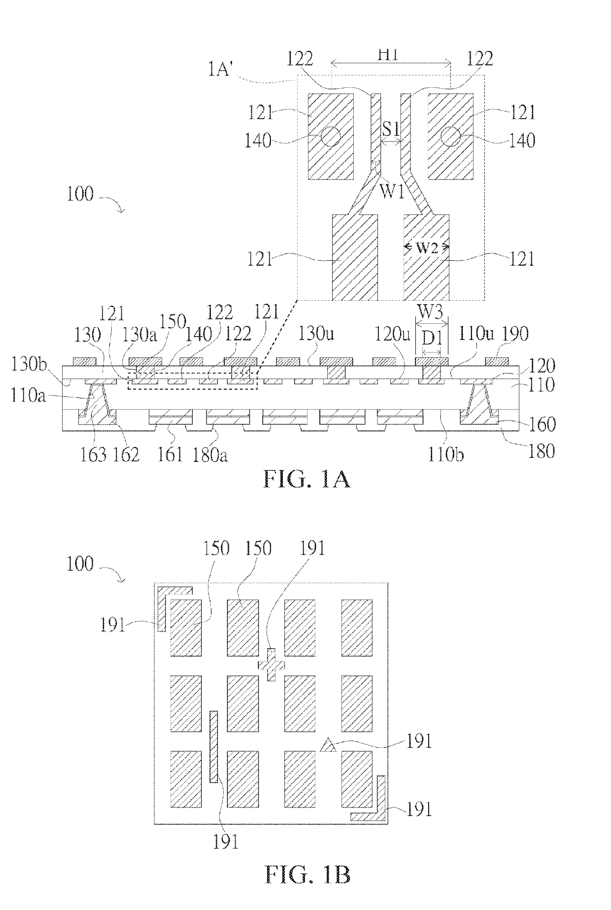
[0025]FIG. 1A is a sectional view of a semiconductor substrate according to an embodiment. A semiconductor substrate 100 includes a dielectric layer 110, a first circuit layer 120, a first protection layer 130, a plurality of first conductive posts 140, a plurality of input / output pads 150, an electrical contact layer 160, a second protection layer 180, and a reinforcing layer 190.
[0026]The dielectric layer 110 is made of, for example, polyimide (PI), a semi-cured sheet of epoxy glass fabric (e.g., prepreg (PP)), or Ajinomoto build-up film (ABF). The dielectric layer 110 has a first surface 110u and a second surface 110b that are opposite to each other.
[0027]The first circuit layer 120 is embedded in the dielectric layer 110 and is exposed from the first surface 110u. Specifically, an end surface 120u of the first circuit layer 120 is exposed from the first surface 110u of the dielectric layer 110. The end surface 120u of the first circuit layer 120 and the first surface 110u of the...
PUM
 Abstract
Description
Claims
Application Information
 - R&D
- Intellectual Property
- Life Sciences
- Materials
- Tech Scout
- Unparalleled Data Quality
- Higher Quality Content
- 60% Fewer Hallucinations
Browse by: Latest US Patents, China's latest patents, Technical Efficacy Thesaurus, Application Domain, Technology Topic, Popular Technical Reports.
© 2025 PatSnap. All rights reserved.Legal|Privacy policy|Modern Slavery Act Transparency Statement|Sitemap|About US| Contact US: help@patsnap.com