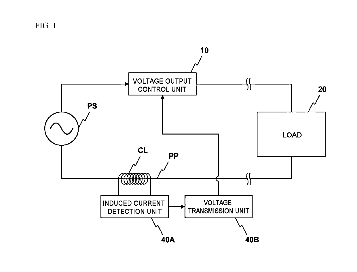
Current detection device having multi-layered PCB core structure
- Summary
- Abstract
- Description
- Claims
- Application Information
AI Technical Summary
Benefits of technology
Problems solved by technology
Method used
Image

Examples
first embodiment
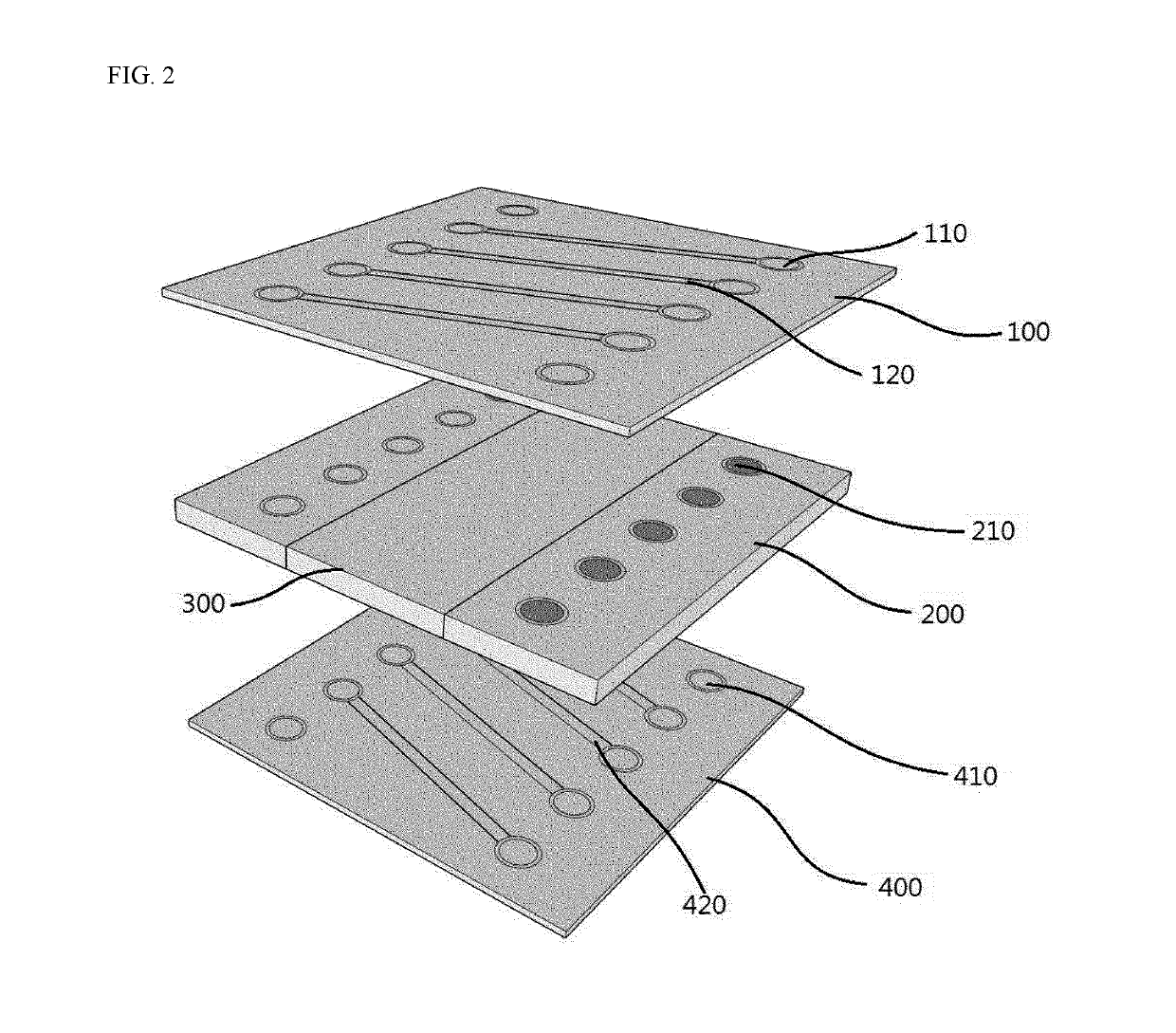
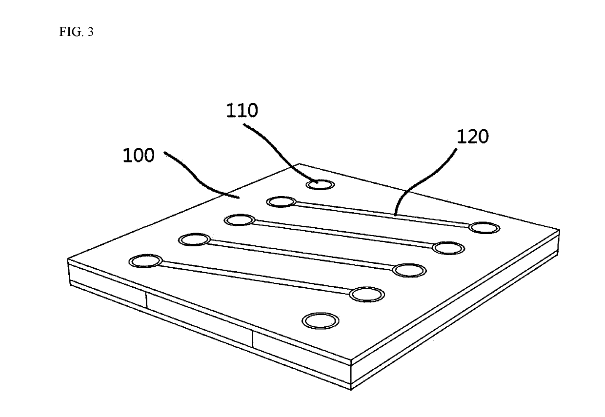
[0048]FIG. 2 is a perspective view illustrating a current detection device having a multi-layered PCB core structure, the layers of which are stacked, according to the present invention. FIG. 3 is a stacked exemplary view.
[0049]As illustrated in FIGS. 2 and 3, the current detection device having a multi-layered PCB core structure includes, from the top, an upper coil pattern forming layer (100), through-hole layers (200), a central core layer (300) formed on the same horizontal line as the through-hole layers, and a lower coil pattern forming layer (400).
[0050]The upper coil pattern foiling layer (100) is made of a nonmagnetic material and has a plurality of coil patterns (120) connected alternately from top to bottom and vice versa through via holes (110).
[0051]The through-hole layers (200) are positioned beneath the upper coil pattern forming layer with the central core layer interposed therebetween, and are horizontal to both sides of the central core layer.
[0052]In this case, ea...
second embodiment
[0058]FIG. 4 is a perspective view illustrating a current detection device having a multi-layered PCB core structure, the layers of which are stacked, according to the present invention. FIG. 5 is a stacked exemplary view.
[0059]FIGS. 6 and 7 are top views illustrating a state in which the layers of the current detection device having a multi-layered PCB core structure according to the second embodiment of the present invention are stacked.
[0060]As illustrated in FIGS. 4 to 7, the current detection device having a multi-layered PCB core structure according to the second embodiment includes an uppermost outer coil pattern forming layer (500), an inner core section (1000), which includes an upper coil pattern forming layer (100), through-hole layers (200), a central core layer (300), and a lower coil pattern forming layer (400), and a lowermost outer coil pattern forming layer (600).
[0061]The inner core section (1000) is formed between the uppermost outer coil pattern forming layer (50...
PUM
 Abstract
Description
Claims
Application Information
 - R&D
- Intellectual Property
- Life Sciences
- Materials
- Tech Scout
- Unparalleled Data Quality
- Higher Quality Content
- 60% Fewer Hallucinations
Browse by: Latest US Patents, China's latest patents, Technical Efficacy Thesaurus, Application Domain, Technology Topic, Popular Technical Reports.
© 2025 PatSnap. All rights reserved.Legal|Privacy policy|Modern Slavery Act Transparency Statement|Sitemap|About US| Contact US: help@patsnap.com