Check patentability & draft patents in minutes with Patsnap Eureka AI!

Electroluminescent display device

Active Publication Date: 2019-05-30
LG DISPLAY CO LTD
View PDF5 Cites 12 Cited by
  • Summary
  • Abstract
  • Description
  • Claims
  • Application Information

AI Technical Summary

Benefits of technology

The present invention provides an electroluminescent display device that has better light extraction and reliability using an overcoat layer with a micro lens and two different thicknesses of the first electrode. This results in improved performance of the display device.

Problems solved by technology

Thus, there is a problem in that light extraction efficiency of the electroluminescent display device 1 is degraded.

Method used


Image

  • Electroluminescent display device
  • Electroluminescent display device
  • Electroluminescent display device

Examples


first embodiment

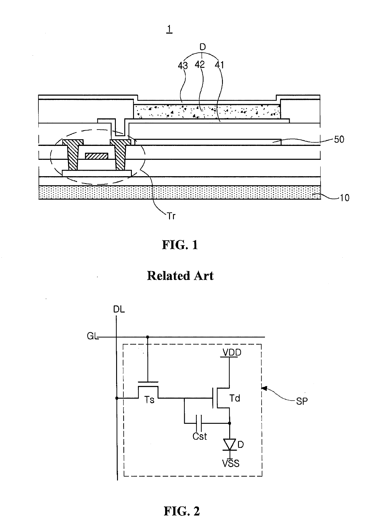
[0029]FIG. 2 is a circuit diagram illustrating a subpixel area of an electroluminescent display device according to an embodiment of the present disclosure.

[0030]As illustrated in FIG. 2, the electroluminescent display device according to the embodiment of the present disclosure includes a gate line GL, a data line DL, a switching thin film transistor Ts, a driving thin film transistor Td, a storage capacitor Cst and a light-emitting diode D. The gate line GL and the data line DL cross each other to define a subpixel area SP. The switching thin film transistor Ts, the driving thin film transistor Td, the storage capacitor Cst and the light-emitting diode D are formed in the subpixel area SP.

[0031]More specifically, a gate electrode of the switching thin film transistor Ts is connected to the gate line GL and a source electrode of the switching thin film transistor Ts is connected to the data line DL. A gate electrode of the driving thin film transistor Td is connected to a drain ele...

second embodiment

[0115]Hereinafter, detailed description of configurations identical or similar to those of the first embodiment may be omitted.

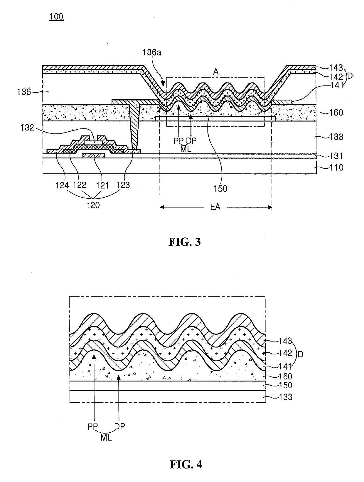
[0116]FIG. 7 is a cross-sectional view schematically illustrating an electroluminescent display device according to a second embodiment of the present disclosure.

[0117]As illustrated in FIG. 7, an electroluminescent display device 200 according to a second embodiment of the present disclosure includes a substrate 210, a thin film transistor 220, a color filter pattern 250, an overcoat layer 260, and a light-emitting diode D electrically connected to the thin film transistor 220.

[0118]The thin film transistor 220 may include a gate electrode 221, an active layer 222, a source electrode 223, and a drain electrode 224.

[0119]Specifically, the gate electrode 221 of the thin film transistor 220 and a gate insulating layer 231 may be disposed on the substrate 210.

[0120]The active layer 222 which overlaps the gate electrode 221 may be disposed on the gate insulating...


PUM


Abstract

An electroluminescent display device comprises a substrate; a thin film transistor disposed on the substrate; an overcoat layer disposed on the thin film transistor; and a light-emitting diode electrically connected to the thin film transistor through the overcoat layer, wherein the light-emitting diode includes a first electrode, a light-emitting layer on the first electrode and a second electrode on the light-emitting layer, and an emissive area is an area in which the light-emitting layer emits light by the first electrode or the second electrode, wherein the overcoat layer includes a micro lens at a position corresponding to the emissive area, and the light-emitting diode conforms to a morphology of the micro lens, and wherein the first electrode includes a first region and a second region, the first region comprises an electrode layer, and the second region includes the electrode layer and an electrode pattern disposed under the electrode layer.

Description

CROSS-REFERENCE TO RELATED APPLICATIONS[0001]This application claims the benefit under 35 U.S.C. § 119(a) of Korean Patent Application No. 2017-0163169, filed Nov. 30, 2017, in the Korean Intellectual Property Office, which is incorporated herein by reference in its entirety.BACKGROUNDTechnical Field[0002]The present disclosure relates to an electroluminescent display device, and more particularly, to an electroluminescent display device capable of improving light extraction efficiency and reliability.Description of the Related Art[0003]In recent years, flat panel displays having excellent characteristics such as being thin, lightweight, and having low power consumption have been widely developed and applied to various fields.[0004]Among the flat panel displays, an electroluminescent display device is a device in which electrical charge carriers are injected into a light-emitting layer formed between a cathode, which is an electron-injecting electrode, and an anode, which is a hole-...

Claims


Application Information

Patent Timeline
IPC IPC(8): H01L51/52H01L51/50H01L27/32
CPCH01L51/5275H01L51/502H01L51/5206H01L51/5221H01L27/322H01L27/3246H01L27/15H01L33/44H01L33/58H01L33/38H10K59/38H10K59/124H10K50/115H10K50/813H10K50/822H10K50/858H10K2102/351H10K50/805H10K50/11H10K50/844H10K50/81H10K50/82H10K59/122
Inventor JO, SO-YOUNGJANG, JI-HYANGCHOI, MIN-GEUNYOUN, WOO-RAM
Owner LG DISPLAY CO LTD
Features
  • R&D
  • Intellectual Property
  • Life Sciences
  • Materials
  • Tech Scout
  • Unparalleled Data Quality
  • Higher Quality Content
  • 60% Fewer Hallucinations
Learn More