Supercharge Your Innovation With Domain-Expert AI Agents!

Multi-way cache expansion circuit architecture

a multi-way cache expansion and circuit technology, applied in the field of computer memory architecture, can solve problems such as exacerbated problems and trade-offs between speed and cos

Inactive Publication Date: 2000-11-14
MICRON TECH INC
View PDF11 Cites 14 Cited by
  • Summary
  • Abstract
  • Description
  • Claims
  • Application Information

AI Technical Summary

Problems solved by technology

The problem is exacerbated by the fact that memory arrays having a high density, which typically makes them less expensive then memory arrays having a lower density, are often slower than memory arrays which have a lower density.
Thus, there is always a trade off between speed and cost.

Method used


Image

  • Multi-way cache expansion circuit architecture
  • Multi-way cache expansion circuit architecture
  • Multi-way cache expansion circuit architecture

Examples


Embodiment Construction

hereinbelow.

For the present invention to be clearly understood and readily practiced, the present invention will be described in conjunction with the following figures wherein:

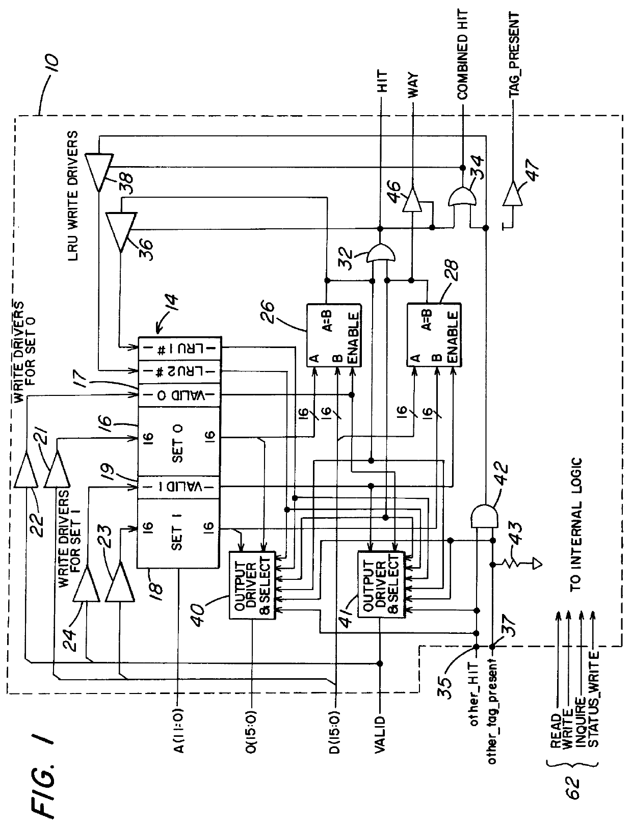
FIG. 1 illustrates an expandable-set, tag, cache circuit constructed according to the teachings of the present invention and implementing a two-way, set associative cache;

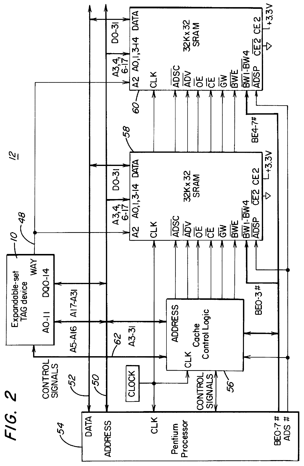
FIG. 2 is a block diagram illustrating a single, expandable-set, cache circuit shown in a cache subsystem;

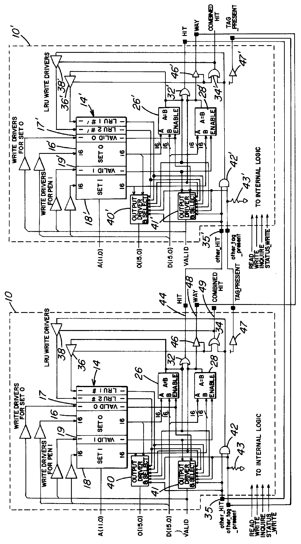
FIG. 3 illustrates the circuit of FIG. 1 connected to implement a four-way, set associative cache; and

FIG. 4 illustrates the output driver and select circuits.

In FIG. 1, an expandable set, tag, cache circuit 10 constructed according to the teachings of the present invention is illustrated. The circuit 10 may be a part of a cache subsystem of a solid state device 12, illustrated in FIG. 2 in block diagram form, which is provided for purposes of illustrating one environment in which the circuit 10 of the present invention may be implemented...


PUM


Abstract

An expandable-set, tag, cache circuit for use with a data cache memory comprises a tag memory divided into a first set and a second set for storing, under a single address location, first and second tag fields representative of first and second data, respectively. The tag memory also stores first and second signals representative of which of the sets is the least recently used. A comparator is responsive to a tag field of an address representative of requested data as well as to a first tag field output from the tag memory for producing an output signal indicative of a match therebetween. A second comparator is responsive to the same tag field of the address and to a second tag field output from the tag memory for producing an output signal indicative of a match therebetween. A first logic gate is responsive to the first and second comparators for producing an output signal indicative of the availability of the requested data in the data cache memory. A second logic gate is responsive to the first logic gate and an external signal. A first write driver is enabled by the output of the first logic gate and is responsive to the output of the first comparator for controlling the state of the first signal. A second write driver is enabled by the output of the second logic gate and is responsive the to external signal for controlling the state of the second signal.

Description

1. Field of the InventionThe present invention relates to the field of computer memory architecture and, more particularly, to cache memories used in conjunction with Static Random Access Memories (SRAM) to improve overall performance.2. Description of the BackgroundThe central processing unit (CPU) of a computer typically operates at a much faster speed than the access time of the memory to which the CPU is connected. The problem is exacerbated by the fact that memory arrays having a high density, which typically makes them less expensive then memory arrays having a lower density, are often slower than memory arrays which have a lower density. Thus, there is always a trade off between speed and cost.To help ameliorate the effects of that trade off, computer designers use both types of memory. The relatively slower memory, which is inexpensive, is used to provide the vast bulk of the memory required and is referred to as the main memory. The more expensive, faster memory, is provide...

Claims


Application Information

Patent Timeline
IPC IPC(8): G06F12/08G06F12/12
CPCG06F12/123G06F12/0864
Inventor PAWLOWSKI, J. THOMAS
Owner MICRON TECH INC
Features
  • R&D
  • Intellectual Property
  • Life Sciences
  • Materials
  • Tech Scout
  • Unparalleled Data Quality
  • Higher Quality Content
  • 60% Fewer Hallucinations
Learn More