Image forming apparatus for making recovery and restoration of toners by electrical conductive member
a technology of electrical conductive members and forming apparatuses, which is applied in the direction of electrographic process apparatuses, instruments, corona discharges, etc., can solve the problems of inability to recover residual developers of transfer devices and inability to obtain excellent image quality
- Summary
- Abstract
- Description
- Claims
- Application Information
AI Technical Summary
Benefits of technology
Problems solved by technology
Method used
Image

Examples
embodiment 1
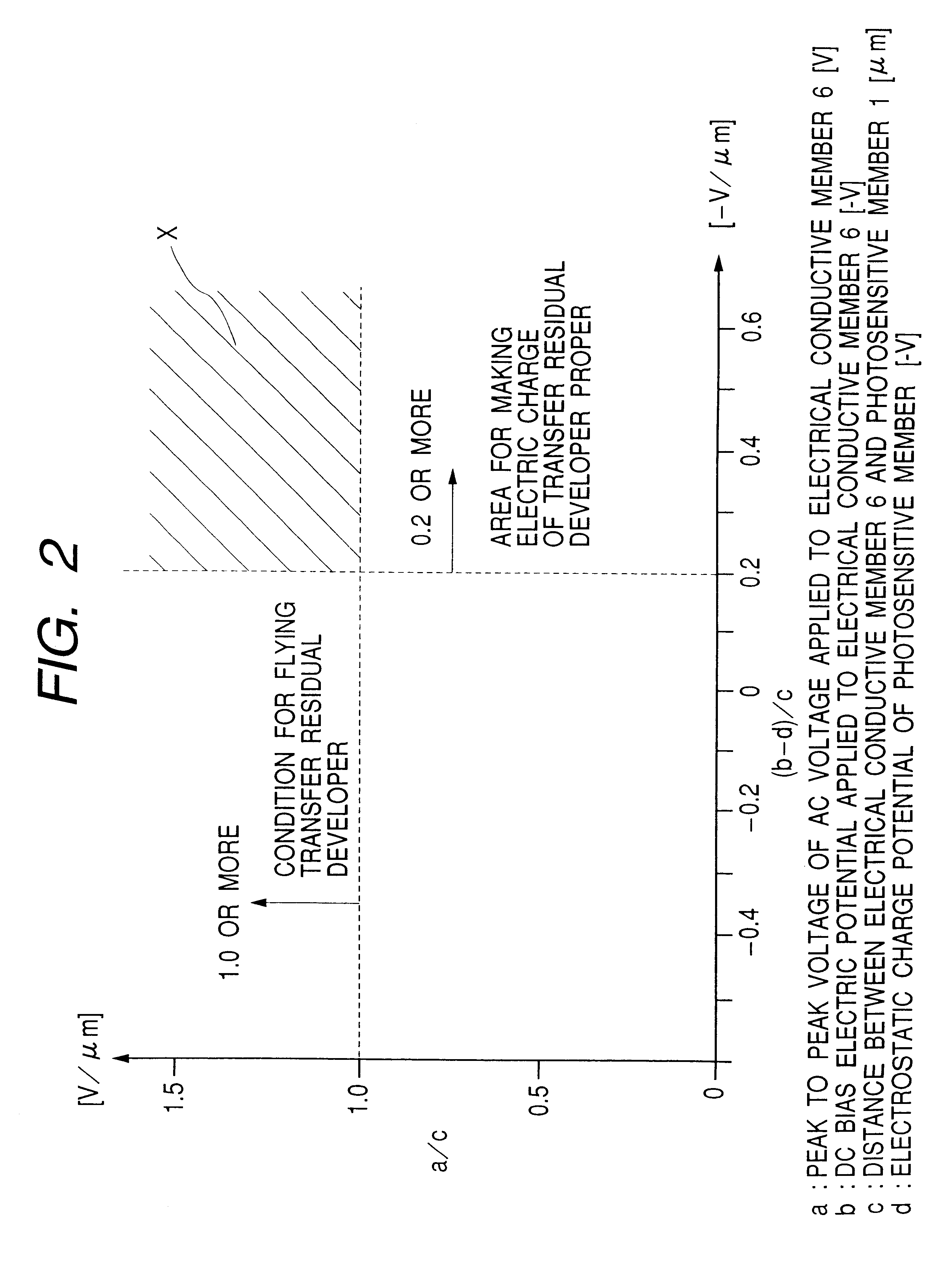
This embodiment is characterized in that it is approximately the same as the embodiment 1 except that the above described (b-d) / c is equal to or less than 0.3[-V / .mu.m].
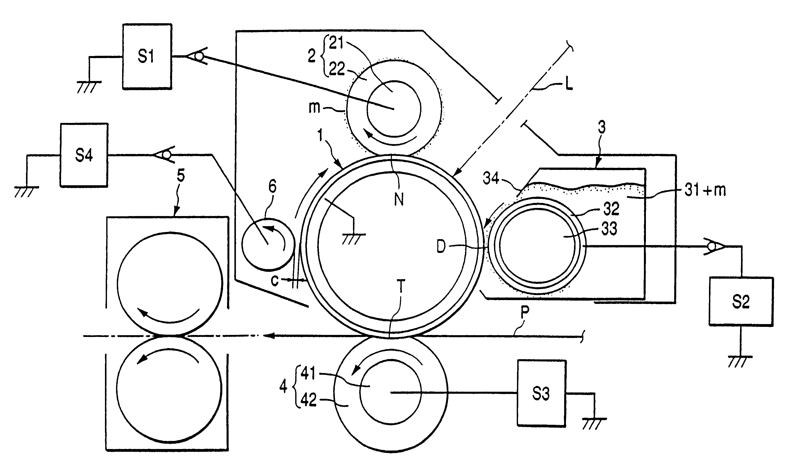
In this manner, the electrification accelerating particles m can be held between the electrical conductive member 6 and the photosensitive member 1 and, for this reason, the electrification accelerating particles m are excessively adhered on the surface of the electrifying roller 2 and the electrification accelerating particle m are prevented from being discharged on the surface of the photosensitive member 1.
In this manner, an excellent electrification property can be maintained and the electrification accelerating particles m adhered to the surface of the photosensitive member 1 are prevented from obstructing the image exposure to adversely affecting the print image.
To be concrete, in this embodiment, the difference between the direct current component potential applied to the electrical conductive member 6 and the...
embodiment 2
The sequence of the DC bias potential for the electrical conductive member 6 is shown in FIG. 5. At the image printing time, similar to the embodiment 2, a rectangular wave having a peak to peak voltage of 1600 V, a frequency of 500 Hz and a DC composition of -800 V is applied and, at the nonprinting time, a rectangular wave having a peak to peak voltage of 1600 V, a frequency of 500 Hz and a DC composition of -900 V is applied.
As shown in FIG. 5, at the image printing time, the DC composition is -800 V, that is, (b-d) / c is 0.24[-V / .mu.m] and, at the nonimage printing time, the DC composition is -900 V, that is, (b-d) / c is 0.44[-V / .mu.m].
In this embodiment, during the image printing time, similar to the embodiment 2, the excessively supplied electrification accelerating particles m are allowed to stay M in the proximity alienating portion c between the electrical conductive member 6 and the photosensitive member 1 as shown in FIG. 3 so that the electrification accelerating particles...
embodiment 4
This embodiment is characterized in that it is approximately the same as the embodiment 4 except that the above described (b-d) / c is equal to or less than 0.3[-V / .mu.m].
In this manner, the electrification accelerating particles m can be held between the electrical conductive member 6 and the electrifying roller 2 and, for this reason, the electrification accelerating particles m are prevented from adhering excessively on the surface of the electrifying roller 2 and being discharged on the surface of the photosensitive member 1.
In this manner, an excellent electrification property can be maintained and the electrifying accelerating particles m adhered to the surface of the photosensitive member 1 are prevented from obstructing the image exposure to adversely affecting the print image.
To be concrete, in this embodiment, the difference between the direct current component potential of the bias applied to the electrical conductive member 6 and the potential applied to the electrifying r...
PUM
 Abstract
Description
Claims
Application Information
 - R&D
- Intellectual Property
- Life Sciences
- Materials
- Tech Scout
- Unparalleled Data Quality
- Higher Quality Content
- 60% Fewer Hallucinations
Browse by: Latest US Patents, China's latest patents, Technical Efficacy Thesaurus, Application Domain, Technology Topic, Popular Technical Reports.
© 2025 PatSnap. All rights reserved.Legal|Privacy policy|Modern Slavery Act Transparency Statement|Sitemap|About US| Contact US: help@patsnap.com