Method of forming CMOS imager with storage capacitor
a technology of cmos imager and storage capacitor, which is applied in the direction of capacitors, diodes, radiation control devices, etc., can solve the problems of high power dissipation of large arrays, ccd imagers also suffer from a number, and are susceptible to radiation damage, so as to improve the storage of collected charges
- Summary
- Abstract
- Description
- Claims
- Application Information
AI Technical Summary
Benefits of technology
Problems solved by technology
Method used
Image
Examples
first embodiment
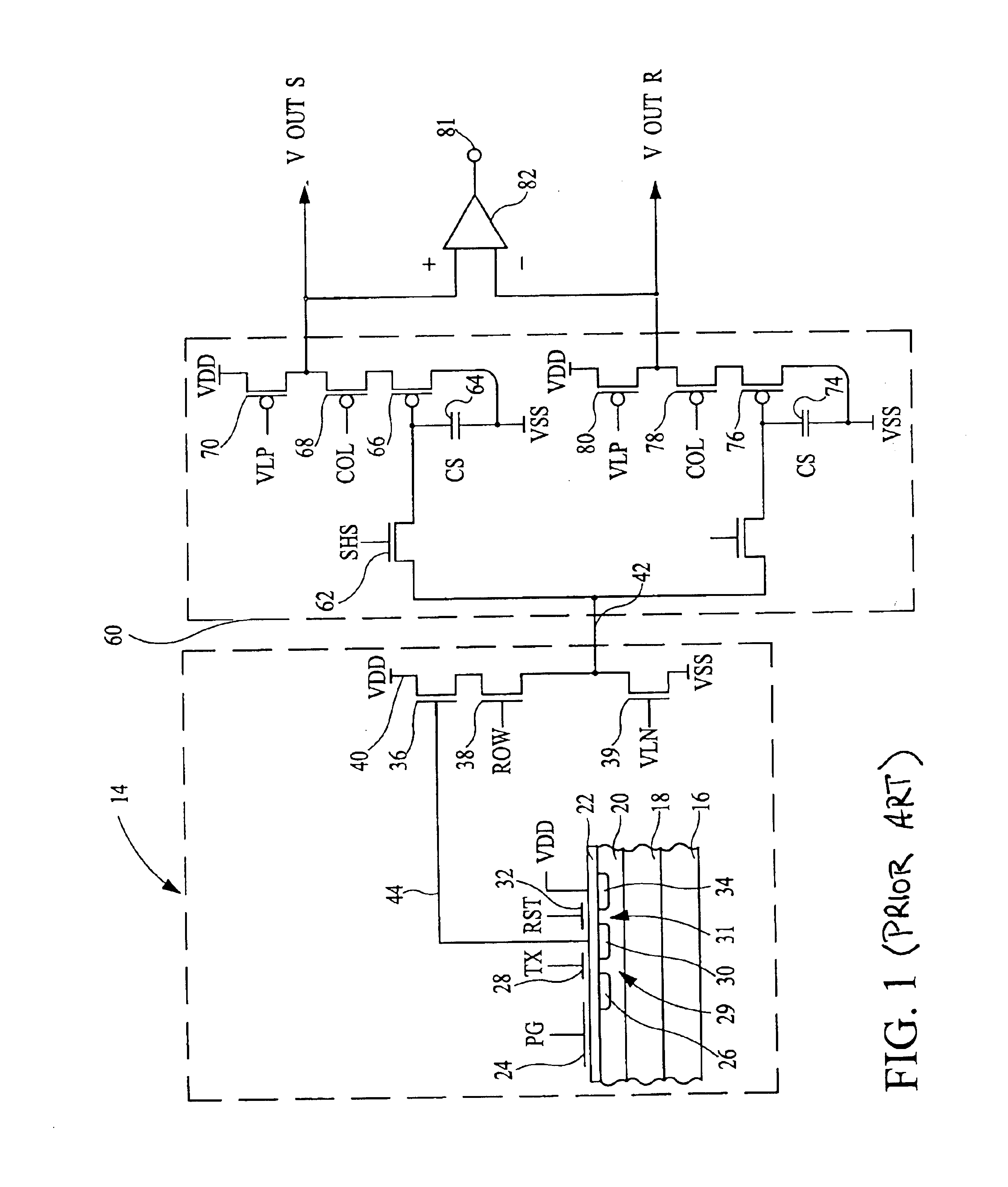
The structure of the pixel cell 114 of a first embodiment is shown in more detail in FIG. 5. The pixel cell 114 may be formed in a substrate 116 having a doped layer 120 of a first conductivity type, which for exemplary purposes is treated as a p-type substrate. A field oxide layer 115, which serves to surround and isolate the cells may be formed by thermal oxidation of the doped layer 120, or by chemical vapor deposition of an oxide material. This field oxide layer 115 may be formed before or after the gate stacks (described below) are formed. The doped layer 120 is provided with five doped regions 110, 126, 130, 134 and 155, which are doped to a second conductivity type, which for exemplary purposes is treated as n type. The first doped region 110 underlies photogate 102, which is a thin layer of material transparent to radiant energy, such as polysilicon. The second doped region 126 electrically connects photogate transistor 125 to the transfer transistor gate 128. An insulating ...
second embodiment
The structure of a pixel cell of the present invention is shown in FIG. 15. The pixel cell 314 may be formed in a substrate 316 having a doped layer 320 of a first conductivity type, which for exemplary purposes is treated as a p-type substrate. A field oxide layer 315, which serves to surround and isolate the cells may be formed by thermal oxidation of the doped layer 320, or by chemical vapor deposition of an oxide material. The doped layer 320 is provided with five doped regions 310, 326, 330, 334 and 355, which are doped to a second conductivity type. For exemplary purposes regions 326, 330, 334, and 355 are treated as n+type. The first doped region 310 is formed under photogate 302 to collect charge and may also be doped n+. Second doped region 326 serves to electrically connect the photosite diffusion 310 to the transfer gate transistor 322. An insulating layer 300 of silicon dioxide, silicon nitride, or other suitable material is formed between the photogate 302 and the photo...
third embodiment
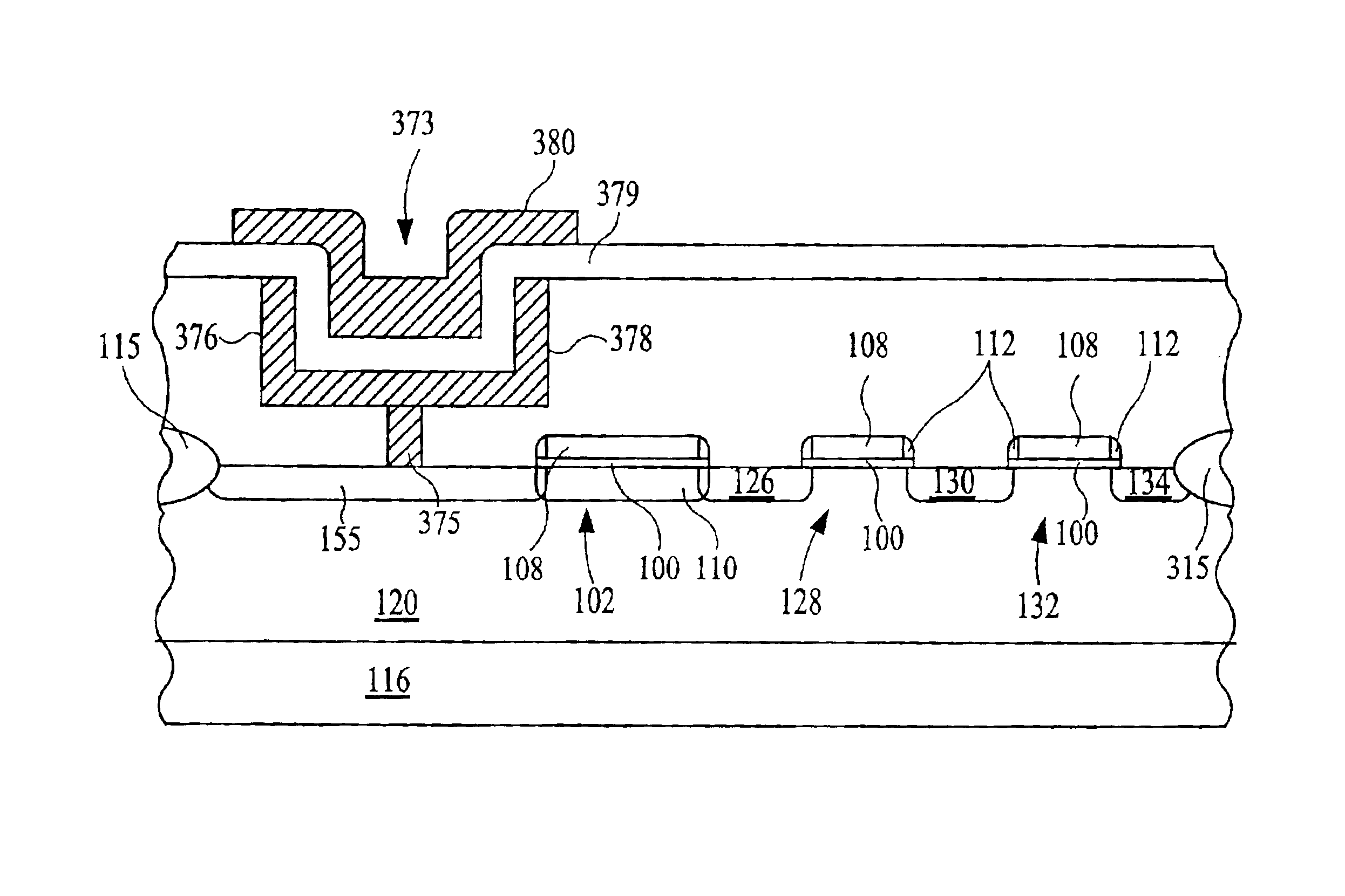
the present invention is described with reference to FIG. 23. It should be understood that similar reference numbers correspond to similar elements as previously described with reference to FIGS. 6-14 and 16-22. The structure set forth in FIG. 23 differs from the above described embodiments in that a stacked storage capacitor 373 is formed in the insulating layer 106 to store charge collected under photogate 102. The processing of the third embodiment is similar to the processing described above with reference to FIGS. 6-9. A hole is etched in the insulating layer 106 down to the fourth doped region 155 and a conductor is formed therein as shown in FIG. 10 to create contact 375; however the etched hole is not fully filled with the conductive material which forms contact 375. The conductor may be formed as a doped polysilicon plug, or as a metallized conductor. A trench 378 is then formed, for example, by etching, in the insulating layer 106 similar to that formed in the substrate as...
PUM
 Abstract
Description
Claims
Application Information
 - R&D Engineer
- R&D Manager
- IP Professional
- Industry Leading Data Capabilities
- Powerful AI technology
- Patent DNA Extraction
Browse by: Latest US Patents, China's latest patents, Technical Efficacy Thesaurus, Application Domain, Technology Topic, Popular Technical Reports.
© 2024 PatSnap. All rights reserved.Legal|Privacy policy|Modern Slavery Act Transparency Statement|Sitemap|About US| Contact US: help@patsnap.com


