Supercharge Your Innovation With Domain-Expert AI Agents!

Liquid crystal display device and method of manufacturing the same

a technology of liquid crystal display and liquid crystal, which is applied in the direction of semiconductor devices, instruments, optics, etc., can solve the problems of poor corrosion resistance of pure aluminum, low production efficiency, and high manufacturing yield of liquid crystal display devices, and achieves low production cost, reduced processing time, and high manufacturing yield

Inactive Publication Date: 2005-03-01
LG DISPLAY CO LTD
View PDF7 Cites 8 Cited by
  • Summary
  • Abstract
  • Description
  • Claims
  • Application Information

AI Technical Summary

Benefits of technology

This approach decreases processing time, increases manufacturing yield, and reduces production costs by simplifying the mask process to four masks, while improving contact resistance between the pixel electrode and the gate pad through side contact.

Problems solved by technology

A process for manufacturing the LCD device described above is very complex.
Pure aluminum has bad corrosion resistance and may cause a line defect due to a hillock in a subsequent process.
If the portion of the ohmic contact layer 54 over the gate electrode 26 is not etched, it produces undesirable electrical characteristics and poor performance of the TFT “S”.
Therefore, even a reduction of one mask results in a shorter processing time, low production costs and high manufacturing yields.

Method used


Image

  • Liquid crystal display device and method of manufacturing the same
  • Liquid crystal display device and method of manufacturing the same
  • Liquid crystal display device and method of manufacturing the same

Examples


Embodiment Construction

Reference will now be made in detail to preferred embodiments of the present invention, examples of which are illustrated in the accompanying drawings.

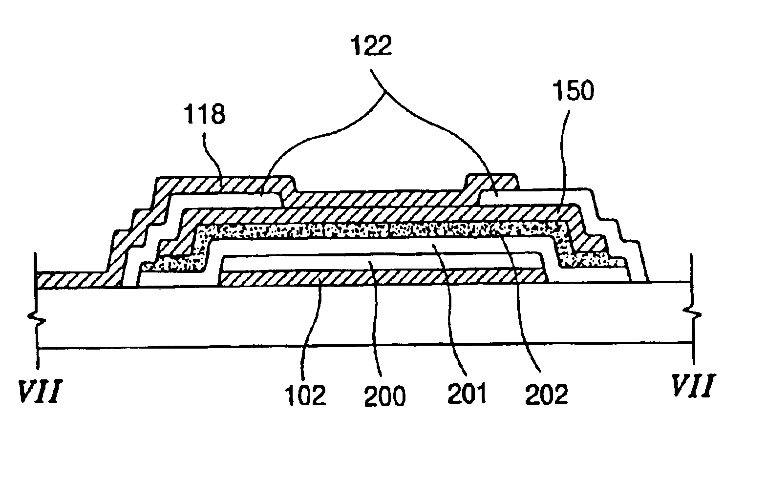
FIG. 4 is a plan view illustrating a lower array substrate of a liquid crystal display (LCD) device according to a preferred embodiment of the present invention. As shown in FIG. 4, gate lines 102 are arranged in a transverse direction and data lines 120 are arranged in a longitudinal direction perpendicular to the gate lines 102. The TFTs are arranged near a crossing point of the gate and data lines 102 and 120. The pixel electrodes 118 are arranged on a region defined by the gate and data lines 102 and 120. Each of the TFT includes a gate electrode 101, a source electrode 112 and the drain electrode 114. The gate electrode 101 extends from the gate line 102, and the source electrode 112 extends from the data line 120. The drain electrode 114 is electrically connected with the pixel electrode 118 through a drain contact hole 116. Dat...


PUM

PropertyMeasurementUnit
liquidaaaaaaaaaa
coloraaaaaaaaaa
colorsaaaaaaaaaa

Abstract

A liquid crystal display, and a method of manufacturing thereof, includes providing a substrate; depositing sequentially a first metal layer and a first insulating layer on the substrate; patterning the first metal layer and the first insulating layer using a first mask to form a gate line and a first gate insulating layer; depositing sequentially a second gate insulating layer, a pure semiconductor layer, a doped semiconductor layer and a second metal layer over the whole substrate; patterning the second metal layer using a second mask to form a data line, source and drain electrodes, a capacitor electrode, the capacitor electrode overlapping a portion of the gae line; etching the doped semiconductor layer between the source and drain electrodes to form a channel region; depositing a third insulating layer over the whole substrate; patterning the third insulating layer using a third mask to form a passivation film, the passivation film having a smaller width than the data line and covering the source and drain electrodes and exposing a portion of the drain electrode and the capacitor electrode; depositing a transparent conductive material layer over the whole substrate; and patterning the transparent conductive material layer using a fourth mask to pixel electrode, the pixel electrode contacting the drain electrode.

Description

BACKGROUND OF THE INVENTION1. Field of the InventionThe present invention relates to a liquid crystal display device, and more particularly, to a liquid crystal display (LCD) device and a method of manufacturing the same.2. Description of Related ArtFIG. 1 is a cross sectional view illustrating a typical LCD device. As shown in FIG. 1, the LCD device includes lower and upper substrates 2 and 4 with a liquid crystal layer 10 interposed therebetween. The lower substrate 2 has a thin film transistor “S” (TFT) as a switching element and a pixel electrode 14, and the upper substrate 4 has a color filter 8 and a common electrode 12. The pixel electrode 14 is formed over a pixel region “P” serves to apply a voltage to the liquid crystal layer 10 along with the common electrode 12, and the color filter 8 serves to implement natural colors. A sealant 6 seals an edge of the lower and upper substrate 2 and 4 to prevent leakage of the liquid crystal.FIG. 2 is a plan view illustrating the lower ...

Claims


Application Information

Patent Timeline
Patent Type & Authority Patents(United States)
IPC IPC(8): G02F1/13G02F1/1362G02F1/136
CPCG02F1/13458G02F1/136227G02F1/136213G02F1/136
Inventor AHN, BYUNG-CHULYOO, SOON-SUNGKIM, YONG-WAN
Owner LG DISPLAY CO LTD
Features
  • R&D
  • Intellectual Property
  • Life Sciences
  • Materials
  • Tech Scout
  • Unparalleled Data Quality
  • Higher Quality Content
  • 60% Fewer Hallucinations
Learn More