Supercharge Your Innovation With Domain-Expert AI Agents!

Custom clock interconnects on a standardized silicon platform

a technology of silicon platform and clock interconnection, applied in the field of integrated circuits, can solve the problems of affecting design costs, risks and time-to-market schedules, and difficult balance between custom features and standard features, and achieve the effects of superior performance in manufacturing tests, clocking functionality, and timing closur

Inactive Publication Date: 2005-06-21
BELL SEMICON LLC
View PDF1 Cites 13 Cited by
  • Summary
  • Abstract
  • Description
  • Claims
  • Application Information

AI Technical Summary

Benefits of technology

This approach enables the creation of standardized clock and reset circuits that are compatible with manufacturing test tools, facilitating faster design completion and reducing technical risks by providing known good clock functions and improving timing closure, thus enhancing the overall performance and efficiency of the chip design process.

Problems solved by technology

The balance between use of standard and custom features is a difficult one that affects design costs, risks and time-to-market schedules and is often based on market forces that set performance requirements, unit costs, volume and design life for the finished integrated chip.
Because the “building blocks” for this technology are system gates or other medium scale logic elements, the complexity that can be achieved is limited.
The design process is long because of the ever-increasing complexity associated with the open-ended nature of this process.
The time needed to integrate and customize the standardized silicon platform is small in comparison to ASIC technology.
Within the entire design space, one area that can cause great difficulty across the spectrum of design activities is the generation, management, qualification and testing of clocking and reset circuitry.
It is found however, that in many cases the clock and reset circuitry is done in a way that is not compatible with the capabilities of the design systems available.
There are many ways to create and manage these circuits poorly.
As a result, they are often not able to meet complex clocking requirements that are unique to each customer's application.
In addition, if these circuits are designed outside the capabilities of the design system, severe delays can be and are encountered in the overall development of the circuit.
Implementation of complex “ad hoc” clock and reset circuitry is often difficult to test using EDA tools, slows down the circuit design process, and introduces considerable technical risk into the performance of the chip.
The “ad hoc” circuitry is difficult to test using standard manufacturing test software tools, leaving potential open loop timing closure problems in the design.

Method used


Image

  • Custom clock interconnects on a standardized silicon platform
  • Custom clock interconnects on a standardized silicon platform
  • Custom clock interconnects on a standardized silicon platform

Examples


Embodiment Construction

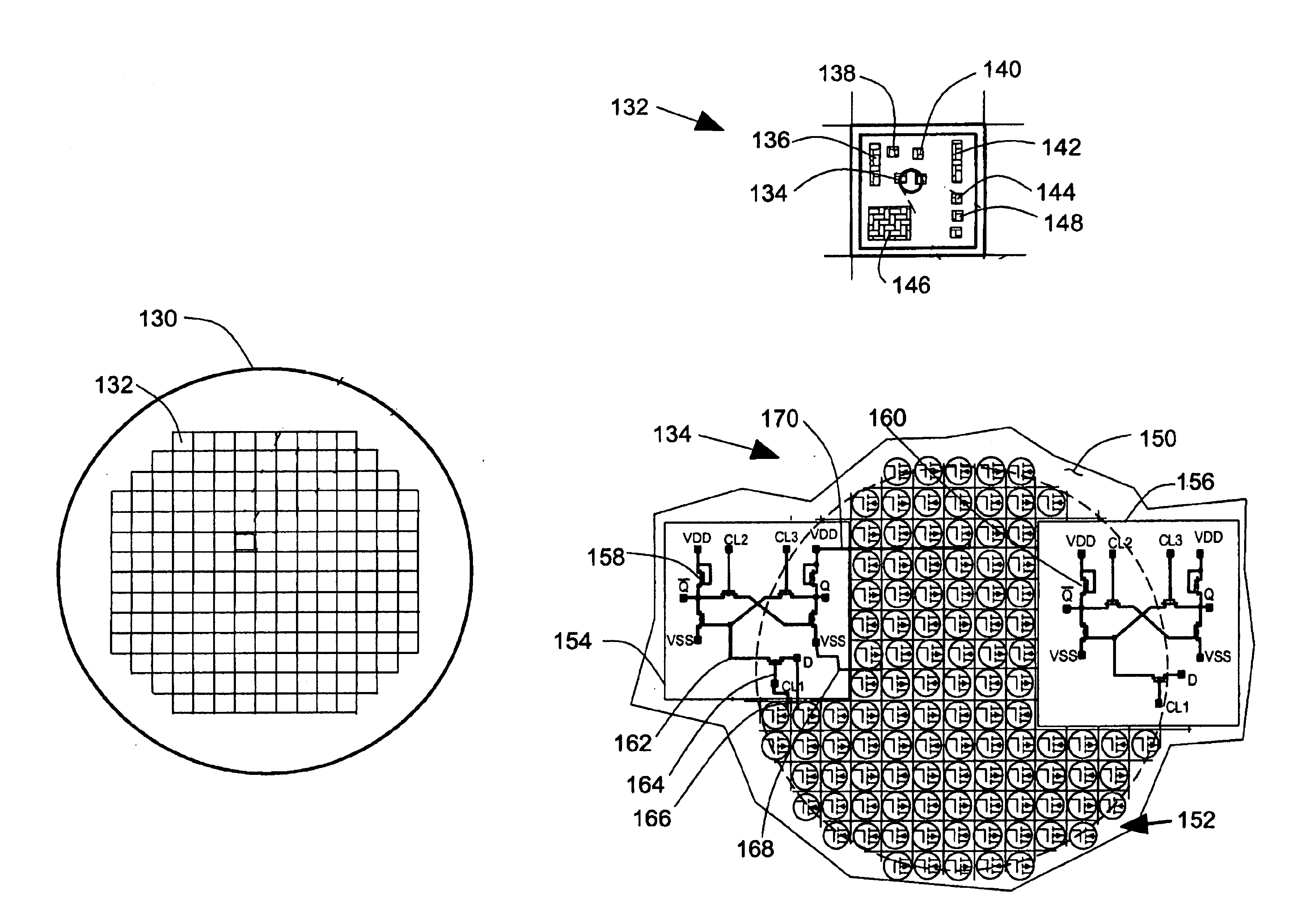
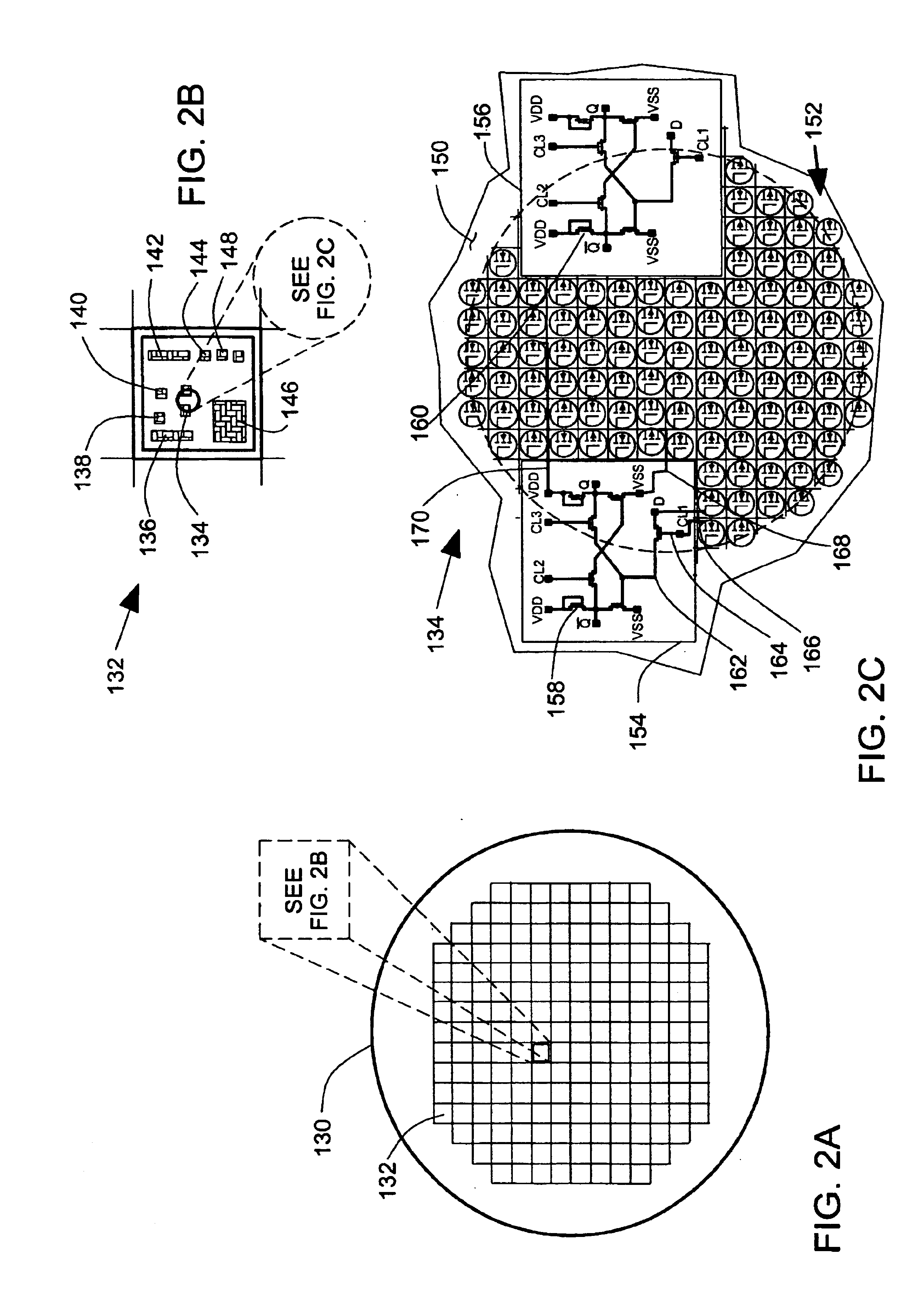
[0021]In the embodiments described below in FIGS. 2-4, a standardized silicon platform design technology is enhanced to include a method and apparatus for the creation of clocking and reset circuits with clock resources such as standard clock factories, standard oscillator sources and standard reset sources. Using a software design tool, the user can customize the clock resources to adapt them to the needs of a custom chip design specification. The use of complex, time consuming, risky add-ons of “ad hoc” circuitry is avoided. Once the custom design is quickly completed using the method and apparatus as expressed in a software design tool, this step of the chip is completed and ready to be passed on for design completion at the manufacturer.

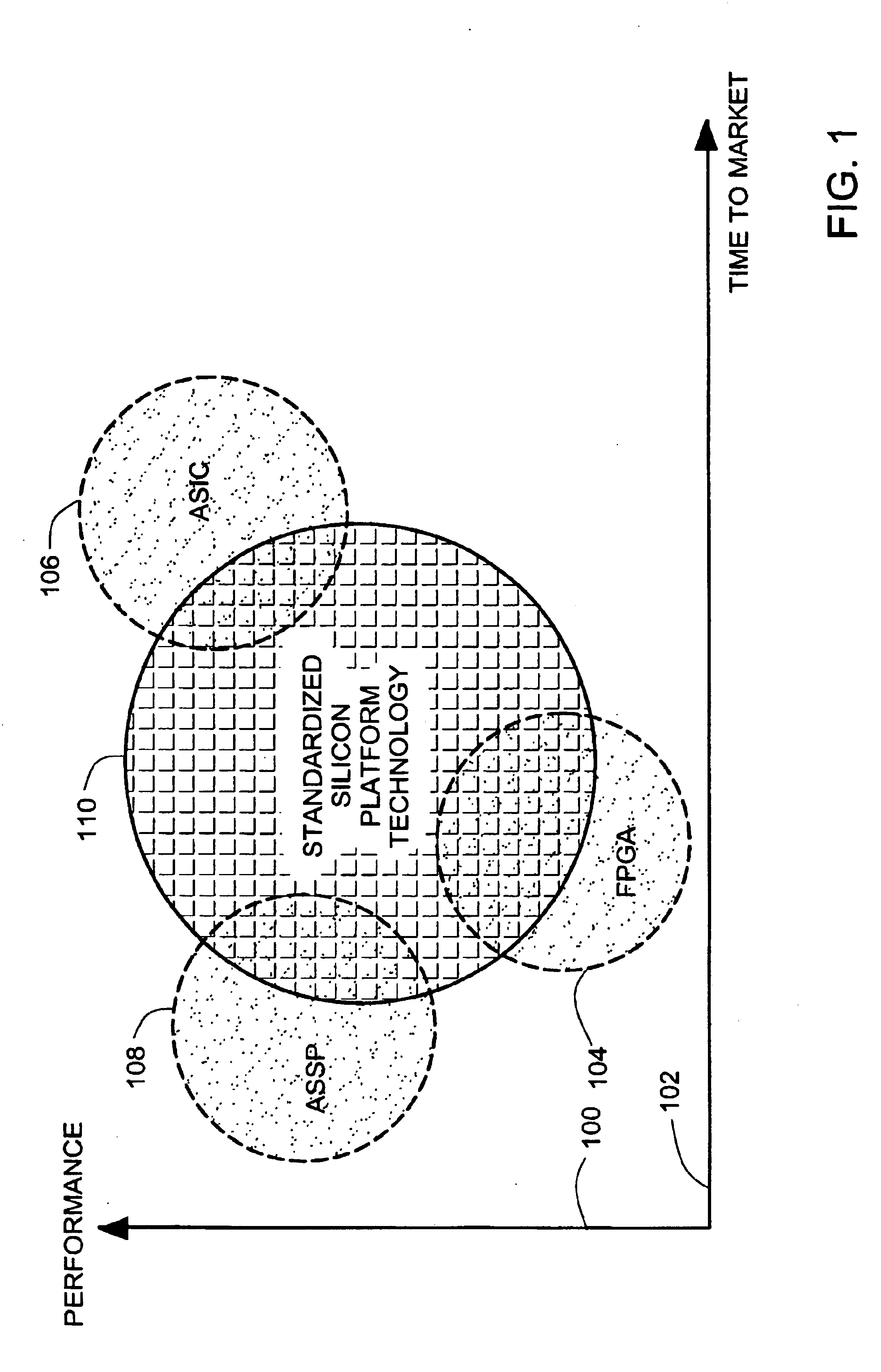
[0022]FIG. 1 (discussed above in the background of the invention) defines the “standardized silicon platform technology” in a context of older technologies such as FPGA, ASIC and ASSP, which it can supplant. Standardized silicon platform technolo...


PUM


Abstract

A standardized silicon platform chip has a substrate surface with an array of unconnected transistors that surround islands. The islands have circuit elements that are interconnectable within each island to form a plurality of varied circuit functions for each of the islands. The varied circuit functions include both application functions and clock functions. Interconnect layers are deposited over the substrate surface to interconnect the circuit elements within each island to complete the varied circuit functions. The varied circuit functions include varied levels of integration including at least gates, flip-flops, clock trees, and oscillators. The varied circuit functions are custom connectable to the array of unconnected transistors to form standard clock resources for the standardized silicon platform chip.

Description

FIELD OF THE INVENTION[0001]The present invention relates to integrated circuits. In particular, the present invention relates to generation of clocks and resets in silicon platform chips.BACKGROUND OF THE INVENTION[0002]In design processes for very large scale integration (VLSI) integrated circuit chips, standard features and custom features can be combined to produce a completed design. The balance between use of standard and custom features is a difficult one that affects design costs, risks and time-to-market schedules and is often based on market forces that set performance requirements, unit costs, volume and design life for the finished integrated chip.[0003]As illustrated in FIG. 1, different design process technologies lead to different mixes of time-to-market and performance. In FIG. 1, a vertical axis 100 represents relative performance in terms of speed and complexity of the functions performed by a chip. A horizontal axis 102 represents relative time lengths of the desi...

Claims


Application Information

Patent Timeline
Patent Type & Authority Patents(United States)
IPC IPC(8): G06F17/50H01L27/10H02H3/00H01L27/02
CPCH01L27/0203G06F17/5045G06F30/30
Inventor BYRN, JONATHAN WILLIAMJENSEN, JAMES ARNOLDWINGREN, MATTHEW SCOTT
Owner BELL SEMICON LLC
Features
  • R&D
  • Intellectual Property
  • Life Sciences
  • Materials
  • Tech Scout
  • Unparalleled Data Quality
  • Higher Quality Content
  • 60% Fewer Hallucinations
Learn More