Check patentability & draft patents in minutes with Patsnap Eureka AI!

Method of cross-mapping integrated circuit design formats

a technology of integrated circuit design and cross-mapping, which is applied in the direction of error detection/correction, instruments, and detecting faulty computer hardware, etc., can solve the problem of exacerbated problem, difficult to determine exactly what is causing the defective ic to fail, and unknown actual root cause of leakage curren

Inactive Publication Date: 2005-09-06
TEXAS INSTR INC
View PDF4 Cites 7 Cited by
  • Summary
  • Abstract
  • Description
  • Claims
  • Application Information

AI Technical Summary

Benefits of technology

This approach allows for accurate and efficient probing of ICs by providing precise coordinates for probe placement, reducing interference from adjacent structures and facilitating detailed failure analysis, even in high-density areas, thereby improving the ability to determine the root cause of defects in ICs.

Problems solved by technology

For example, if an IC has a current leakage path on an input / output pin, the pin may be deemed defective, but the actual root cause of the leakage current may still be unknown.
Furthermore, it can be extremely difficult to determine exactly what is causing the defective IC to fail, especially when the IC has been packaged.
IC technology trends only exacerbate this problem, as the number of transistors contained in each successive generation of ICs doubles approximately every eighteen months and more routing layers are required to connect tightly packed circuit elements.
Thus, the particular analysis used to determine the root cause of the problem is commensurate with the nature of the failure since some problems may be determined by testing the packaged IC, and other problems would require testing at the surface of the IC.
Furthermore, the pins 14 of the flip-chip package 16 are in the form of conductive metal balls that span across the bottom of the package 16, so simply removing the bottom of the packaging to gain access to the circuitry with a micro-mechanical probe is impossible without completely removing the IC 10 from the flip-chip package 16, which is impractical.
Nevertheless, although the ability to probe any desired point is satisfied using an optical microscope / probe, finding the desired point in the IC to direct the probe to can still be like finding a needle in a haystack because physical access to the frontside of the IC is not available for viewing and navigating the optical probe.
In addition, although the optical probe is capable of producing an image of the IC through the backside, often this image is not detailed enough to use in navigating the IC while looking for the desired probe point.
This problem is only exacerbated by the millions of devices integrated in today's ICs, and thus, navigating the optical probe from an imprecise image can make it difficult to locate and probe the desired point.
However, correlating between the point of interest on the CAD representation or “road map” and the actual IC in a non-flip-chip arrangement can be difficult because of the density of the electrical devices, and can be even more difficult in a flip-chip packaging arrangement because of the imprecise image obtained from the optical probe as described above.
In addition to encountering problems, With optical probing arrangements, navigating through the various integrated structures in an IC using other probing methods can be problematic also.
For example, invasive probing techniques using fine probing needles (e.g., on the order of 1 μm) may not be able to probe down to desired probe points on the IC because of interference from adjacent integrated structures, such as metal routing layers.
This can be especially problematic in high-density areas of the IC, and becomes more problematic with each successive version of ICs as more routing layers are used.

Method used


Image

  • Method of cross-mapping integrated circuit design formats
  • Method of cross-mapping integrated circuit design formats
  • Method of cross-mapping integrated circuit design formats

Examples


Embodiment Construction

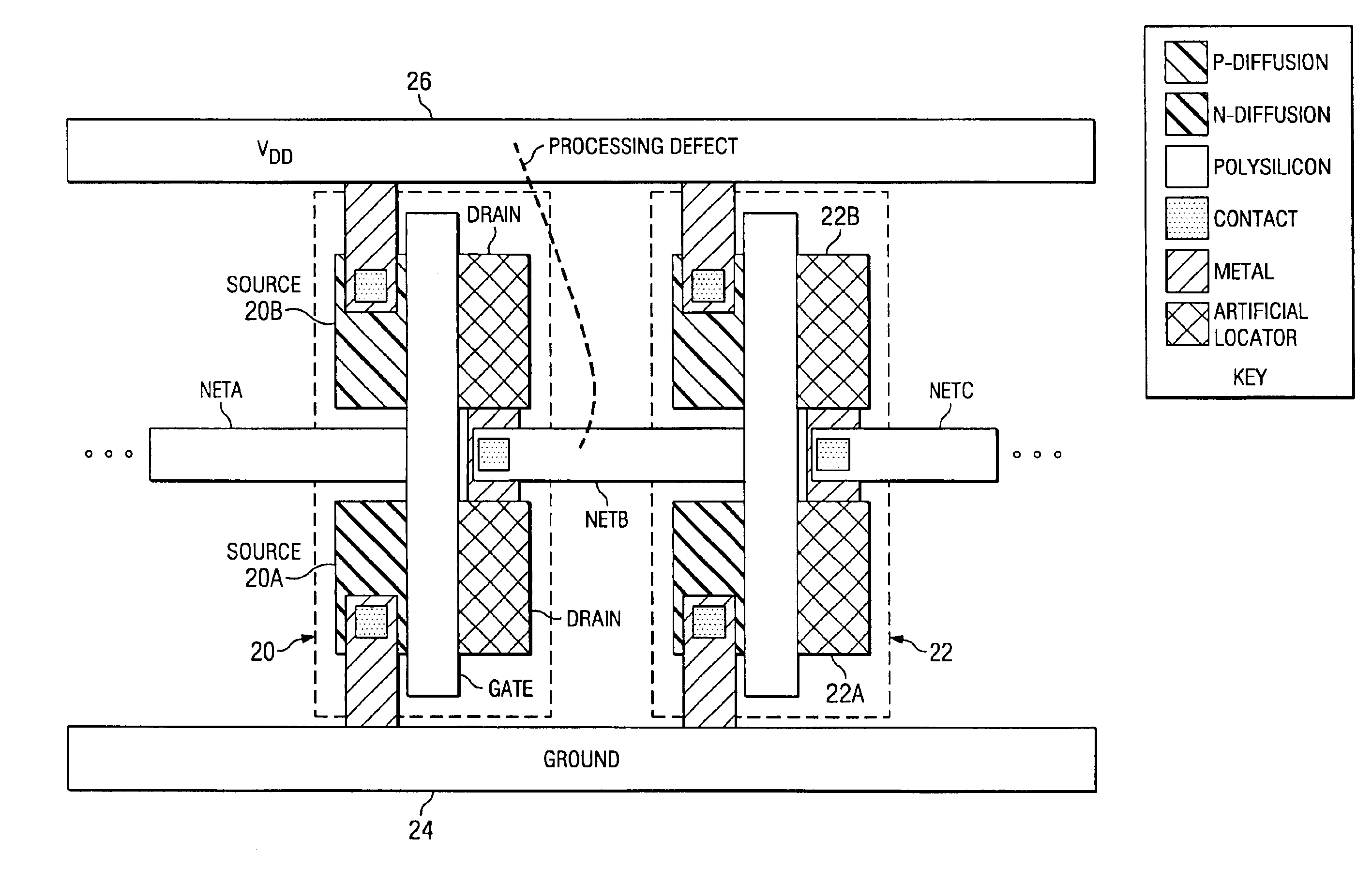
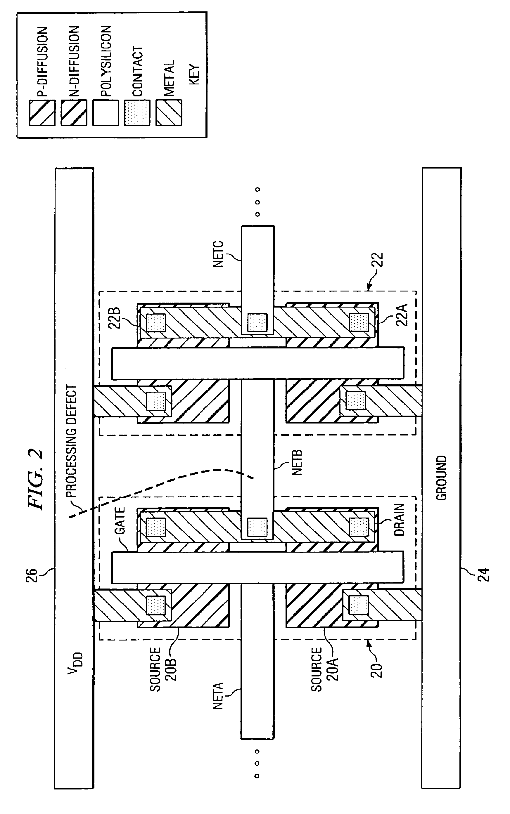
[0013]The problems noted above in large part are addressed by using “artificial locator cells” to cross-map the coordinates from the layout view of the IC and provide probe locations with minimal interference from adjacent structures. An artificial locator cell refers to a cell that is deliberately placed into the CAD representation, but is not used in fabricating the IC. In one embodiment the different layers of the layout have different computational functions performed on them in order to furnish possible probe points. For example, the polysilicon layer and the diffusion layer may have the NAND function performed on them so that the result generates polygons that represent the drain and source regions of MOSFETs. Alternatively, the polysilicon and diffusion layers may have mathematical operations performed on them such that the coordinates of where the two layers abut are revealed for probing. Nets used to interconnect circuit elements (e.g., logic gates, transistors, resistors, ...


PUM


Abstract

A method of cross-mapping integrated circuit (“IC”) elements nets in a IC and / or directing a probe to points on an IC to achieve minimal interference from adjacent structures is disclosed. The method of provides a more streamlined approach than referencing points from a physical layout representation of the IC to the actual IC being tested. The improved correlation between the actual packaged IC and the layout of the IC is accomplished using artificial locator cells. Preferably, the artificial locator cells are generated from mathematical operations of the extracted version of the layout, and they further provide coordinate information for where minimal interference from adjacent structures may be accomplished. Artificial locator cells may be generated from a layout representing a hierarchical representation or alternately each element that is instantiated from a reference library may already have artificial locator cells included.

Description

CROSS-REFERENCE TO RELATED APPLICATIONS[0001]Not applicable.STATEMENT REGARDING FEDERALLY SPONSORED RESEARCH OR DEVELOPMENT[0002]Not applicable.BACKGROUND OF THE INVENTION[0003]1. Field of the Invention[0004]The present invention generally relates to integrated circuit design. More particularly, the invention relates to techniques for cross-mapping integrated circuit design formats.[0005]2. Background Information[0006]The ubiquitous presence of integrated circuits (“ICs”) in almost every electronic device is testament to their importance in today's society. An integral part of producing ICs is “failure analysis,” which is the determination of why product failure is occurring. For example, if an IC has a current leakage path on an input / output pin, the pin may be deemed defective, but the actual root cause of the leakage current may still be unknown. Furthermore, it can be extremely difficult to determine exactly what is causing the defective IC to fail, especially when the IC has be...

Claims


Application Information

Patent Timeline
Patent Type & Authority Patents(United States)
IPC IPC(8): G06F17/50G01R31/317
CPCG01R31/31707G01R31/31718G06F17/5081G06F30/398
Inventor JOSHI, HEMANTTHOMAS, DAVID A.BACH, JOHNCARAWAN, RAND B.
Owner TEXAS INSTR INC
Features
  • R&D
  • Intellectual Property
  • Life Sciences
  • Materials
  • Tech Scout
  • Unparalleled Data Quality
  • Higher Quality Content
  • 60% Fewer Hallucinations
Learn More