Supercharge Your Innovation With Domain-Expert AI Agents!

Switchable capacitance and nonvolatile memory device using the same

a technology of nonvolatile memory and capacitance, which is applied in the direction of digital storage, semiconductor devices, instruments, etc., can solve the problems of unsatisfactory power consumption and manufacturing costs for many applications, and achieve the effects of reducing manufacturing costs, reducing power consumption, and fast switching speeds

Inactive Publication Date: 2006-01-24
INT BUSINESS MASCH CORP
View PDF8 Cites 8 Cited by
  • Summary
  • Abstract
  • Description
  • Claims
  • Application Information

AI Technical Summary

Benefits of technology

This approach enables faster switching speeds, lower power consumption, and potentially lower manufacturing costs, with the switching member persisting in its conductivity state until reversed, offering improved performance over existing technologies.

Problems solved by technology

The above-mentioned devices provide switching speeds, power consumptions and manufacturing costs which are still unsatisfactory for many applications.

Method used


Image

  • Switchable capacitance and nonvolatile memory device using the same
  • Switchable capacitance and nonvolatile memory device using the same
  • Switchable capacitance and nonvolatile memory device using the same

Examples


Embodiment Construction

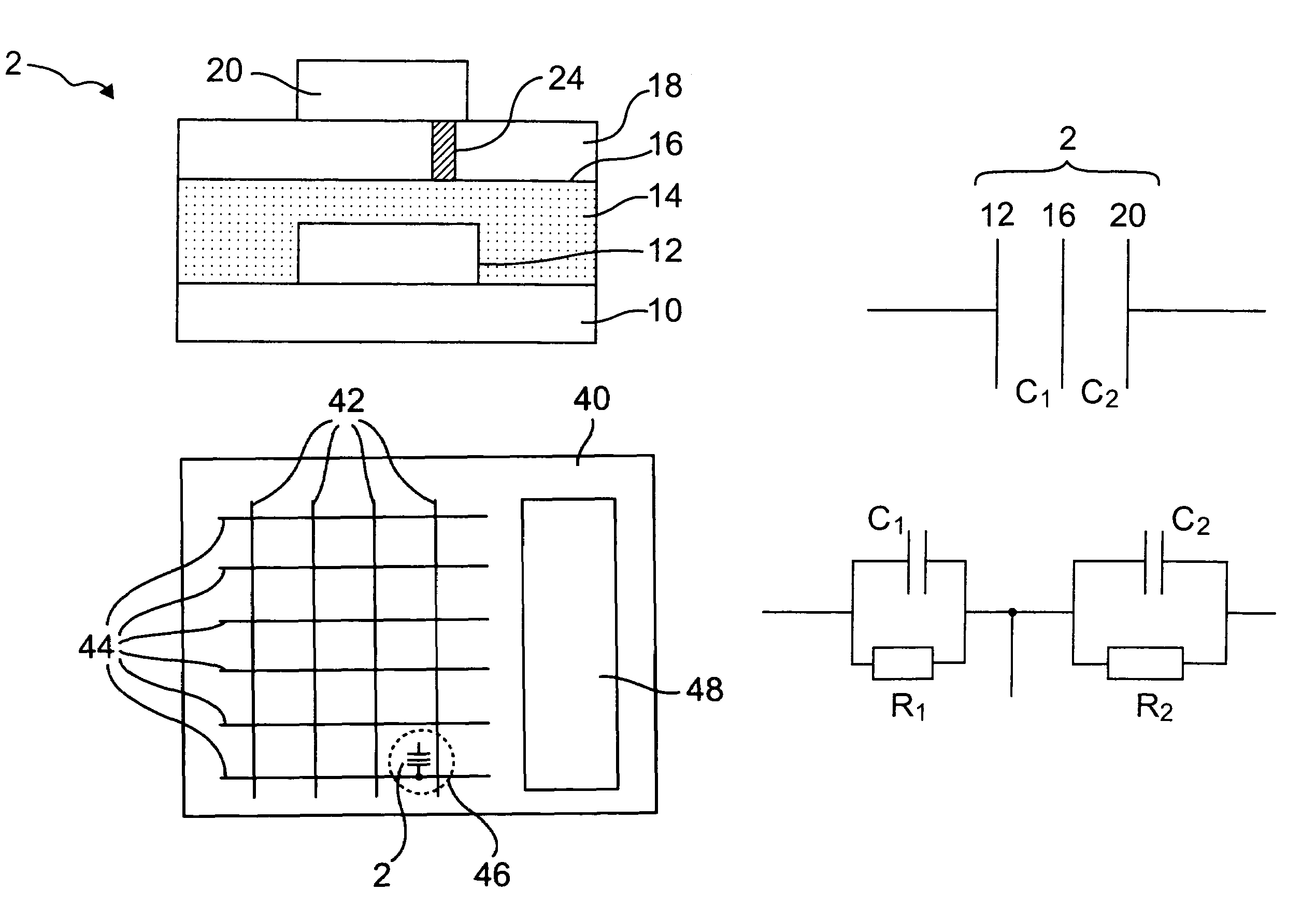
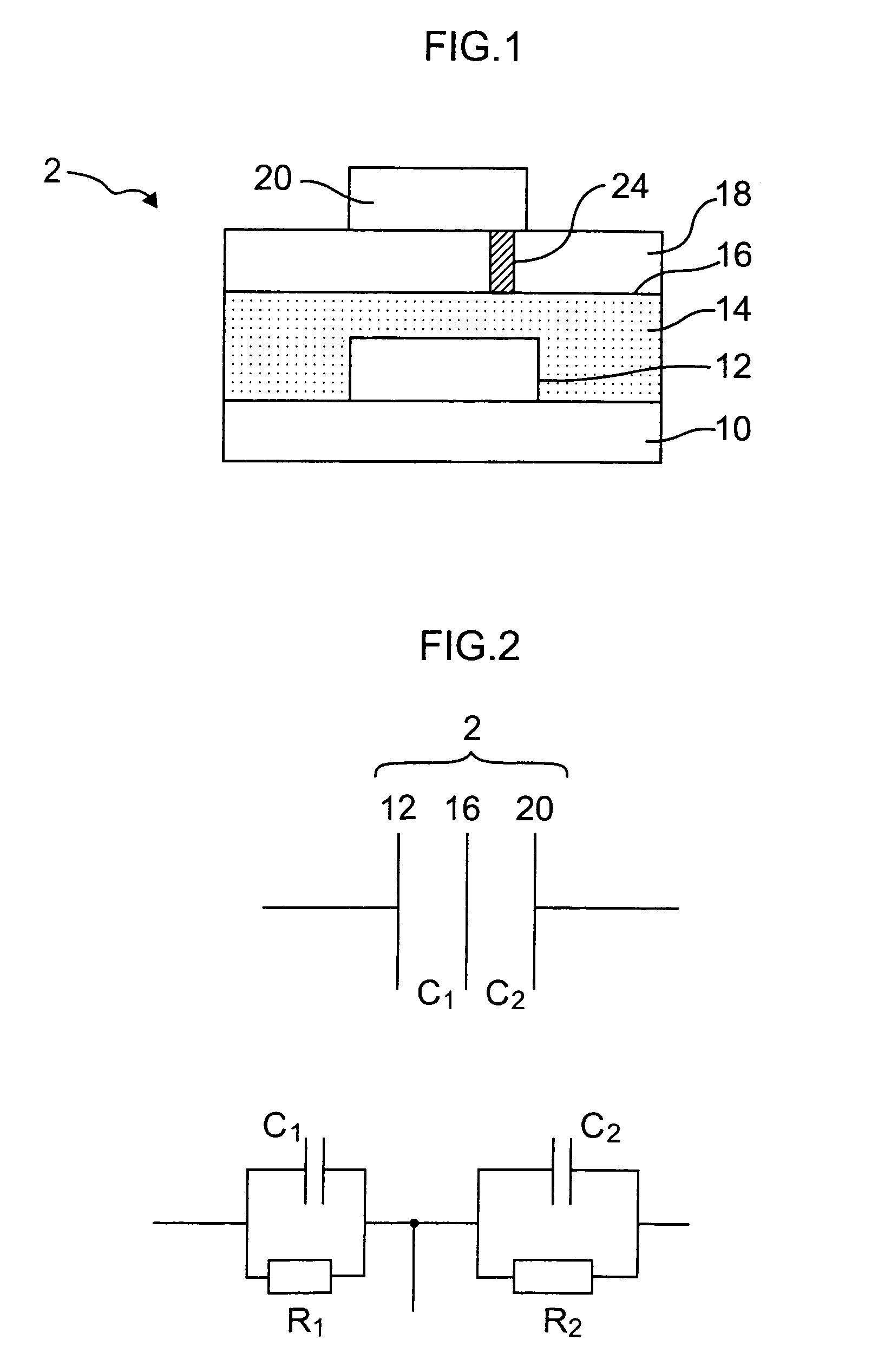
[0029]FIG. 1 is a schematic sectional view of a capacitor 2 according to a first preferred embodiment of the present invention. On a substrate 10, a stack-like arrangement of a first capacitor electrode 12, a dielectric layer 14, an intermediate layer 16, a switching member 18 and a second capacitor electrode 20 is formed. The first capacitor electrode 12 and the second capacitor electrode 20 are herein also referred to as first electrode 12 and second electrode 20, respectively. The first capacitor electrode 12 and the second capacitor electrode 20 and the intermediate electrode 16 between the capacitor electrodes 12, 20 are essentially in parallel to each other and separated from each other by the dielectric layer 14 and the switching member 18, respectively. The first capacitor electrode 12, the intermediate electrode 16 and the second capacitor electrode 20 at least partially overlap, and preferentially at least the capacitor electrode 12, 20 essentially completely overlap. This...


PUM


Abstract

A device (2) with a switchable capacitance comprises a first and a second electrode (12, 20) facing each other, a dielectric layer (14) between a first and a second capacitor electrode (12, 20), and a switching member (18) between the second electrode (20) and the dielectric layer (14), the switching member (18) comprising a switching material reversibly switchable between a lower conductivity state and a higher conductivity state, each of the lower conductivity state and the higher conductivity state being persistent, wherein the capacitance of the device (2) depends on the conductivity state of the switching material.

Description

BACKGROUND OF THE INVENTION[0001]1. Field of the Invention[0002]The present invention refers to a device with a capacitance that can be switched between at least two different values and to a non-volatile memory device using the same.[0003]2. Description of the Related Art[0004]For memory devices and for numerous other applications, bistable devices or circuits are used. For example, for storing one bit of information in a memory, a bistable device can be used which is switchable between (at least) two different and persistent states. When writing a logical “1” into the device, it is driven into one of the two persistant states and when writing a logical “0” or erasing the logical “1”, the device is driven into the other of the two different states. Each of the states persists until a next step of writing information into the device or erasing information in the device proceeds. A huge number of such bistable devices arranged in one or more arrays may form an EEPROM (EEPROM stands f...

Claims


Application Information

Patent Timeline
Patent Type & Authority Patents(United States)
IPC IPC(8): G11C11/24G11C11/22G11C11/34G11C13/00
CPCG11C11/22H01G7/06G11C13/00
Inventor BEDNORZ, GEORG J.GUNDLACH, DAVID J.MEIJER, GERHARD I.RIESS, WALTER H.
Owner INT BUSINESS MASCH CORP
Features
  • R&D
  • Intellectual Property
  • Life Sciences
  • Materials
  • Tech Scout
  • Unparalleled Data Quality
  • Higher Quality Content
  • 60% Fewer Hallucinations
Learn More