Supercharge Your Innovation With Domain-Expert AI Agents!

Solder pad configuration for use in a micro-array integrated circuit package

a micro-array integrated circuit and configuration technology, applied in electrical equipment, semiconductor devices, semiconductor/solid-state device details, etc., can solve the problems of lead-frame based packages, bga packages have drawbacks, and large footprints, so as to improve the shear strength and reliability increase the surface area, and increase the size of the solder joint

Active Publication Date: 2006-08-08
NAT SEMICON CORP
View PDF17 Cites 34 Cited by
  • Summary
  • Abstract
  • Description
  • Claims
  • Application Information

AI Technical Summary

Benefits of technology

[0007]In another embodiment of the invention, a substrate panel for use in the packaging of integrated circuits comprises a lead-frame panel including an array of device areas. Each device area has an array of contacts exposed on the lower surface of the substrate panel, and a plurality of leads extending to sides of the device area. Each lead has an associated contact, wherein at least some of the leads have segments extending between the contacts associated with adjacent leads. The contacts also each have a generally noncircular shape with a geometric center, the generally noncircular shape at least partially defined by a major dimension, in which the generally noncircular shape has a greater surface area than the corresponding surfaces of generally circular shapes with diameters substantially equal to the major dimension. This increased surface area increases the size of, and thus improves the shear strength and reliability of, the solder joint.

Problems solved by technology

Current semiconductor packaging technology often involves tradeoffs between ease and efficiency of manufacturing on the one hand, and various performance drawbacks on the other.
However, lead-frame based packages, whose connectors are typically placed either on or extending from the sides, tend to have larger footprints than ball grid array (BGA) packages, whose solder ball connectors lie directly underneath the package.
Unfortunately, BGA packages have drawbacks as well.
Specifically, such packages often employ laminate substrates rather than uniform metal lead-frames, making them more expensive to produce than lead-frame based packages, and less efficiently manufactured.

Method used


Image

  • Solder pad configuration for use in a micro-array integrated circuit package
  • Solder pad configuration for use in a micro-array integrated circuit package
  • Solder pad configuration for use in a micro-array integrated circuit package

Examples


Embodiment Construction

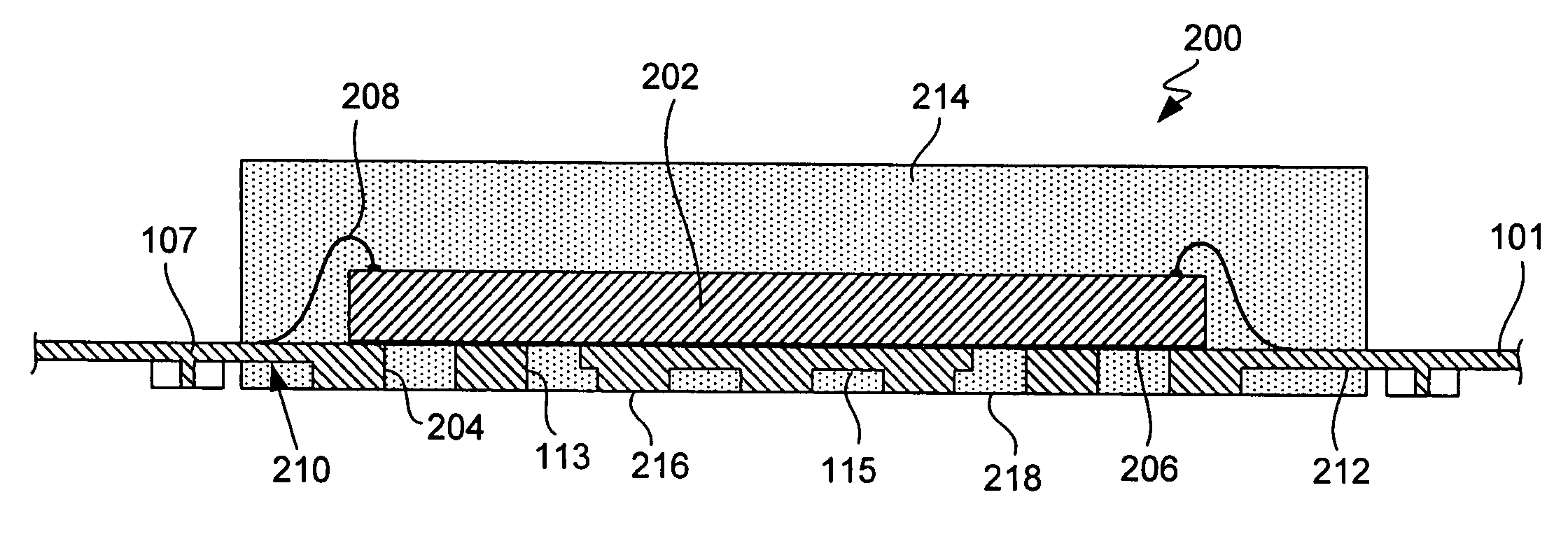
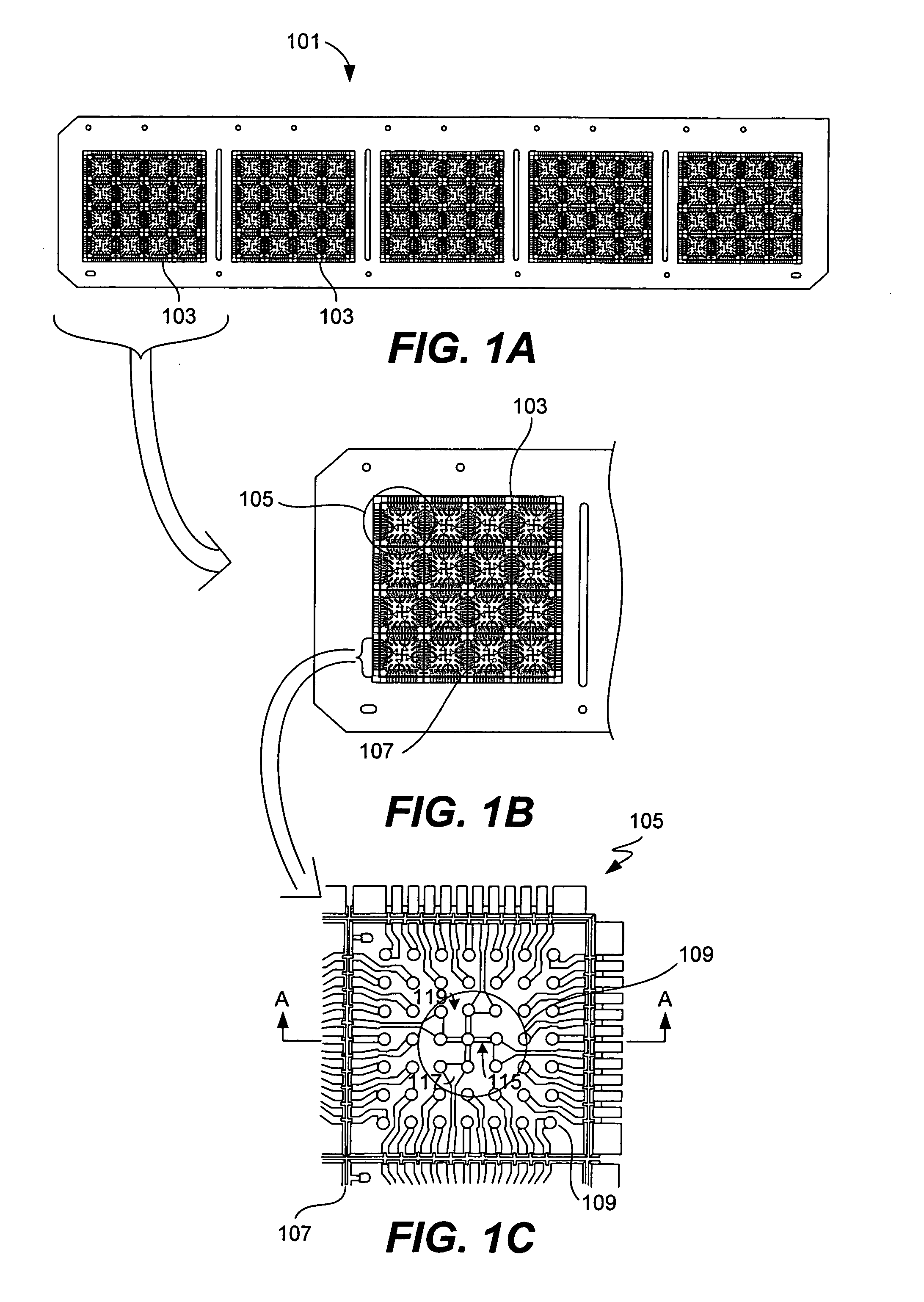
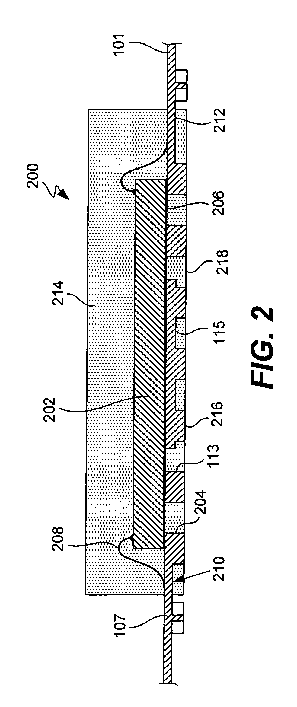
[0019]In one embodiment of the invention, an integrated circuit package is disclosed. The package has solder ball connectors on its lower surface, like conventional BGA packages. However, this package is produced using many features of lead-frame based packages. Such a package utilizes at least four different elements to achieve various improvements over the art. First, a lead-frame is employed with perforated die attach pads that allow encapsulant material to more easily flow underneath the dice, thus preventing process problems such as voids in the encapsulant layer. The drive toward smaller package sizes has also yielded smaller contact pads for placing solder ball connectors. As reductions in contact pad area also reduce the strength with which solder balls adhere to the package, a second improvement involves square contact pads that retain the same metal-to-metal clearance as standard circular contact pads, but that have a greater surface area. In this manner, embodiments of th...


PUM


Abstract

A solder pad configuration for use in an IC package is described. Various embodiments of the invention describe IC packages, lead-frames, or substrate panels configured with generally noncircular solder pads at their bottom surfaces. The noncircular shapes allow for greater surface area than circular solder pads having diameters equal to a major dimension of the noncircular shapes, while maintaining the same metal-to-metal clearance between the pads and adjacent leads. This increased surface area provides for stronger and more reliable solder joints.

Description

BRIEF DESCRIPTION OF THE INVENTION[0001]This invention relates to the packaging of integrated circuits (ICs). More specifically, this invention relates to the design and fabrication of a micro-array IC package.BACKGROUND OF THE INVENTION[0002]Current semiconductor packaging technology often involves tradeoffs between ease and efficiency of manufacturing on the one hand, and various performance drawbacks on the other. For example, lead-frame based packages such as quad flat no-lead (QFN) packages employ lead-frames to facilitate the packaging and singulation of multiple units at once. However, lead-frame based packages, whose connectors are typically placed either on or extending from the sides, tend to have larger footprints than ball grid array (BGA) packages, whose solder ball connectors lie directly underneath the package. Unfortunately, BGA packages have drawbacks as well. Specifically, such packages often employ laminate substrates rather than uniform metal lead-frames, making ...

Claims


Application Information

Patent Timeline
IPC IPC(8): H01L23/495H01L23/04
CPCH01L23/3107H01L23/49541H01L23/49548H01L23/49503H01L24/48H01L2224/48091H01L2224/48247H01L2224/48463H01L2224/73265H01L2924/01013H01L2924/01029H01L2924/01078H01L2924/01079H01L2924/00014H01L2924/14H01L2924/181H01L2224/48257H01L2224/48465H01L2224/97H01L2924/00H01L2924/00012H01L2224/45099H01L2224/45015H01L2924/207
Inventor BAYAN, JAIME A.PRABHU, ASHOK S.LEE, SHAW WEI
Owner NAT SEMICON CORP
Features
  • R&D
  • Intellectual Property
  • Life Sciences
  • Materials
  • Tech Scout
  • Unparalleled Data Quality
  • Higher Quality Content
  • 60% Fewer Hallucinations
Learn More