Supercharge Your Innovation With Domain-Expert AI Agents!

Semiconductor storage device, test method therefor, and test circuit therefor

a technology of semiconductor memory and storage device, which is applied in the direction of digital storage, measurement device, instruments, etc., can solve the problems of increasing power consumption, requiring higher costs than dram, and dram requires more complicated timing control than sram

Inactive Publication Date: 2007-03-20
RENESAS ELECTRONICS CORP
View PDF8 Cites 38 Cited by
  • Summary
  • Abstract
  • Description
  • Claims
  • Application Information

AI Technical Summary

Benefits of technology

Enables thorough testing of semiconductor memory devices to identify and prevent malfunctions caused by short time intervals between read / write and refresh operations, ensuring reliable device performance.

Problems solved by technology

However, since the SRAM generally requires six transistors per memory cell, the chip size becomes large anyhow and it disadvantageously requires higher costs than the DRAM.
Consequently, the DRAM requires more complicated timing control than the SRAM.
Another problem with the DRAM is that the memory cells must be refreshed even when there are no external accesses, which increases power consumption.
Third, the SRAM requires only a small standby current and consumes only low power and is thus suitable for cellular phones, for which it is desired to maximize continuous call time and continuous standby time.
Timings for generating a self-refresh operation cannot be externally controlled.
Consequently, the time intervals for these operations cannot be externally controlled.
Malfunction may occur if the self-refresh operation overlaps the read or write operation.
However, the above measure may not ensure sufficient circuit operations.
For example, if a timing for generating a self-refresh operation is temporarily close to a timing for generating a read or write operation, the operations may interfere with each other to cause malfunction.
The following malfunction may occur: the interference between word lines, an insufficient precharge resulting from short time intervals for operations, or the disturbance of an operation by a pulse signal generated by another operation.
However, these techniques only check the refresh operation itself and does not check how the device will operate if the time interval between a read or write operation and the refresh operation is short.

Method used


Image

  • Semiconductor storage device, test method therefor, and test circuit therefor
  • Semiconductor storage device, test method therefor, and test circuit therefor
  • Semiconductor storage device, test method therefor, and test circuit therefor

Examples


first embodiment

(First Embodiment)

[0090]A first embodiment of the present invention will be described below with reference to the drawings.

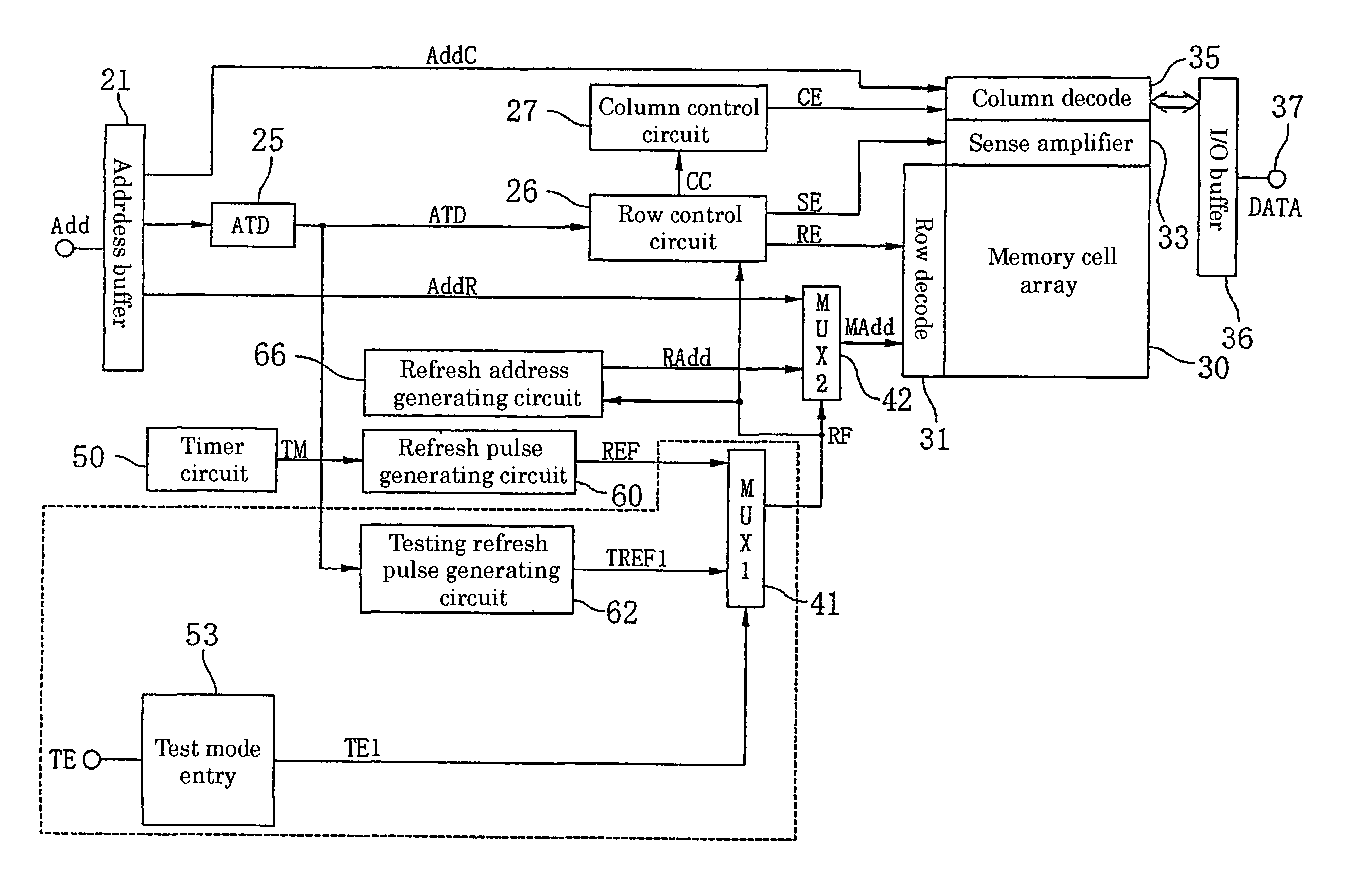
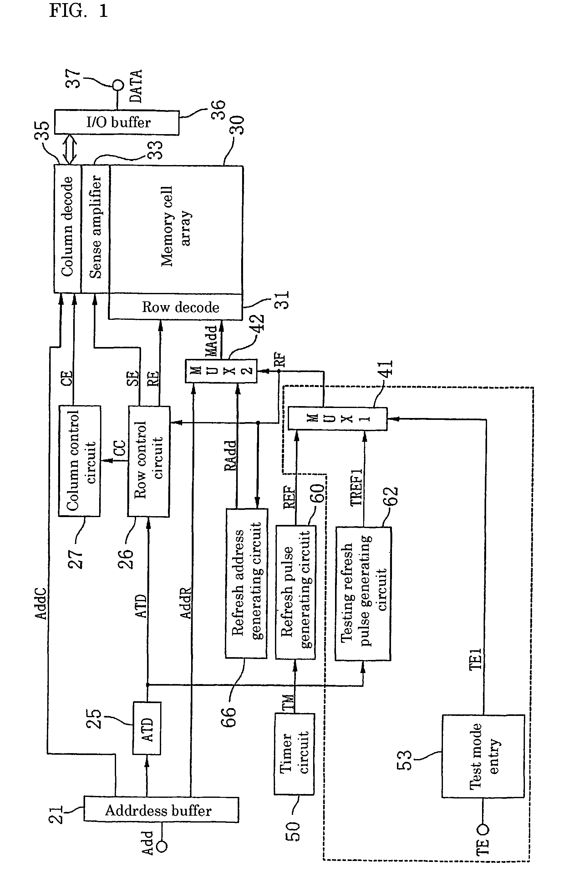
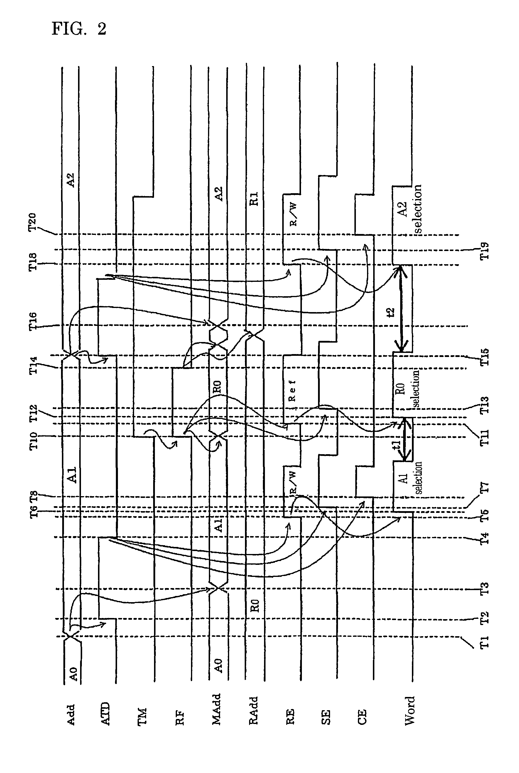
[0091]FIG. 1 is a block diagram showing the circuit configuration of a semiconductor memory device (pseudo SRAM) according to the first embodiment. FIG. 2 is a timing chart showing a normal operation performed by the semiconductor memory device shown in FIG. 1. First, the circuit configuration of the semiconductor memory device (pseudo SRAM) will be described with reference to FIG. 1. With reference to FIG. 2, description will be given of the normal operation performed by the semiconductor memory device according to the present application.

[0092]A read / write address signal Add is externally inputted to an address buffer circuit 21. An address transition detecting circuit (ATD circuit) 25 is connected to the address buffer circuit 21 to receive the read / write address signal Add as an input. When at least one bit in the address data Add changes, the address transi...

second embodiment

(Second Embodiment)

[0164]A second embodiment of the present invention will be described below with reference to the drawings.

[0165]The circuit configuration of a semiconductor memory device according to the present embodiment is the same as that of the semiconductor memory device according to the first embodiment. Moreover, the normal mode operation of the semiconductor memory device according to the present embodiment is the same as that of the semiconductor memory device according to the first embodiment. The semiconductor memory device according to the present embodiment differs from the semiconductor memory device according to the first embodiment only in the test mode operation. Accordingly, the description of the circuit configuration and normal mode operation of the semiconductor memory device according to the present embodiment is omitted. The test mode operation will be described below with reference to FIG. 5. FIG. 5 is a timing chart showing an operation performed in the ...

third embodiment

(Third Embodiment)

[0185]A third embodiment of the present invention will be described below with reference to the drawings.

[0186]The first embodiment generates the first testing refresh pulse signal TREF1 the predetermined time (TA1′) after the address transition detection signal ATD has changed, to set the self refresh operation to be started so that time interval “t1” between this self refresh operation and the preceding read or write operation is shortest. The first embodiment thus carries out tests under the worst timing condition (hereinafter referred to as the “first worst timing condition”). The second embodiment generates the second testing refresh pulse signal TREF2 the predetermined time (TA2′) after a rise of the address transition detection signal ATD, to set the self refresh operation so that time interval “t2” between this self refresh operation and the preceding read or write operation is shortest. The second embodiment thus carries out tests under the worst timing co...


PUM


Abstract

A test method and a test circuit which enable operations to be checked when the time interval between a refresh operation and a read or write operation is forcibly reduced. Timings for a read or write operation in a normal operation mode and in a test mode are determined on the basis of an address transition detection circuit. A timing for a refresh operation in the normal operation mode is set on the basis of a normal refreshing pulse signal generated by a refresh pulse generating circuit in response to a timing signal generated by a timer circuit. A timing for a refresh operation in the test mode is set on the basis of a first testing refresh pulse generation signal generated by a first testing refresh pulse generating circuit in response to the address transition detection signal. By controlling a timing for generating the first testing refresh pulse generation signal, it is possible to generate a read or write operation and a refresh operation so that there is a predetermined time interval between these operations.

Description

[0001]This application is a 371 of PCT / JP02 / 12930 filed Dec. 10, 2002.[0002]1. Technical Field[0003]The present invention relates to a semiconductor memory device and a method of testing the semiconductor memory device, and a test circuit.[0004]2. Background Art[0005]SRAMs and DRAMs are the most typical of randomly accessible semiconductor memory devices. The SRAM generally operates faster than the DRAM. Further, simply by receiving a power supply and an inputted address, an internal sequential circuit can operate in response to this change in address to execute a read or write. The SRAM is thus operated simply by receiving a simple input waveform, in contrast to the DRAM. It is thus possible to simplify a circuit that generates such an input signal waveform.[0006]Further, the SRAM can retain data stored in memory cells without refreshing, in contrast to the DRAM. Thus, advantageously, the SRAM can be easily handled and requires only a small data retention current in a standby state...

Claims


Application Information

Patent Timeline
Patent Type & Authority Patents(United States)
IPC IPC(8): G11C7/00G01R31/28G01R31/3185G11C8/18G11C11/401G11C11/403G11C11/406G11C29/08G11C29/14
CPCG11C8/18G11C29/14G11C29/12015G11C11/406G11C11/401
Inventor TAKAHASHI, HIROYUKIINABA, HIDEOUCHIDA, SYOUZOU
Owner RENESAS ELECTRONICS CORP
Features
  • R&D
  • Intellectual Property
  • Life Sciences
  • Materials
  • Tech Scout
  • Unparalleled Data Quality
  • Higher Quality Content
  • 60% Fewer Hallucinations
Learn More