Check patentability & draft patents in minutes with Patsnap Eureka AI!

Method of fabricating semiconductor device

a semiconductor device and manufacturing method technology, applied in semiconductor/solid-state device manufacturing, transistors, electric devices, etc., can solve the problems of high probability, unfavorable variations of semiconductor device characteristics, and nmos transistors vulnerable to hot carrier generation, and achieve the effect of reducing leakage curren

Active Publication Date: 2007-04-10
COLUMBA TECH INC
View PDF28 Cites 1 Cited by
  • Summary
  • Abstract
  • Description
  • Claims
  • Application Information

AI Technical Summary

Benefits of technology

[0024]An object of the present invention is to provide a method of fabricating a semiconductor device, by which leakage current is reduced in a manner of minimizing electron or hole density in forming a source / drain configuring a P / N junction with a channel area of a transistor.

Problems solved by technology

If such a requirement for the dimensional reduction of the semiconductor device fails to be met, a channel length between source and drain is shortened to result in unfavorable variations of the semiconductor device characteristics such as the short channel effect (SCE).
Yet, since the operational power requested by an electronic product is still high despite the dimensional reduction of the semiconductor device, electrons injected from a source of an NMOS transistor are severely accelerated in a potential gradient state of a drain to make the NMOS transistor vulnerable to hot carrier generation for example.
Moreover, it is highly probable that leakage current is generated from the depletion area by an electric field.

Method used


Image

  • Method of fabricating semiconductor device
  • Method of fabricating semiconductor device
  • Method of fabricating semiconductor device

Examples


Embodiment Construction

[0034]Reference will now be made in detail to the preferred embodiments of the present invention, examples of which are illustrated in the accompanying drawings. Wherever possible, the same reference numbers will be used throughout the drawings to refer to the same or like parts.

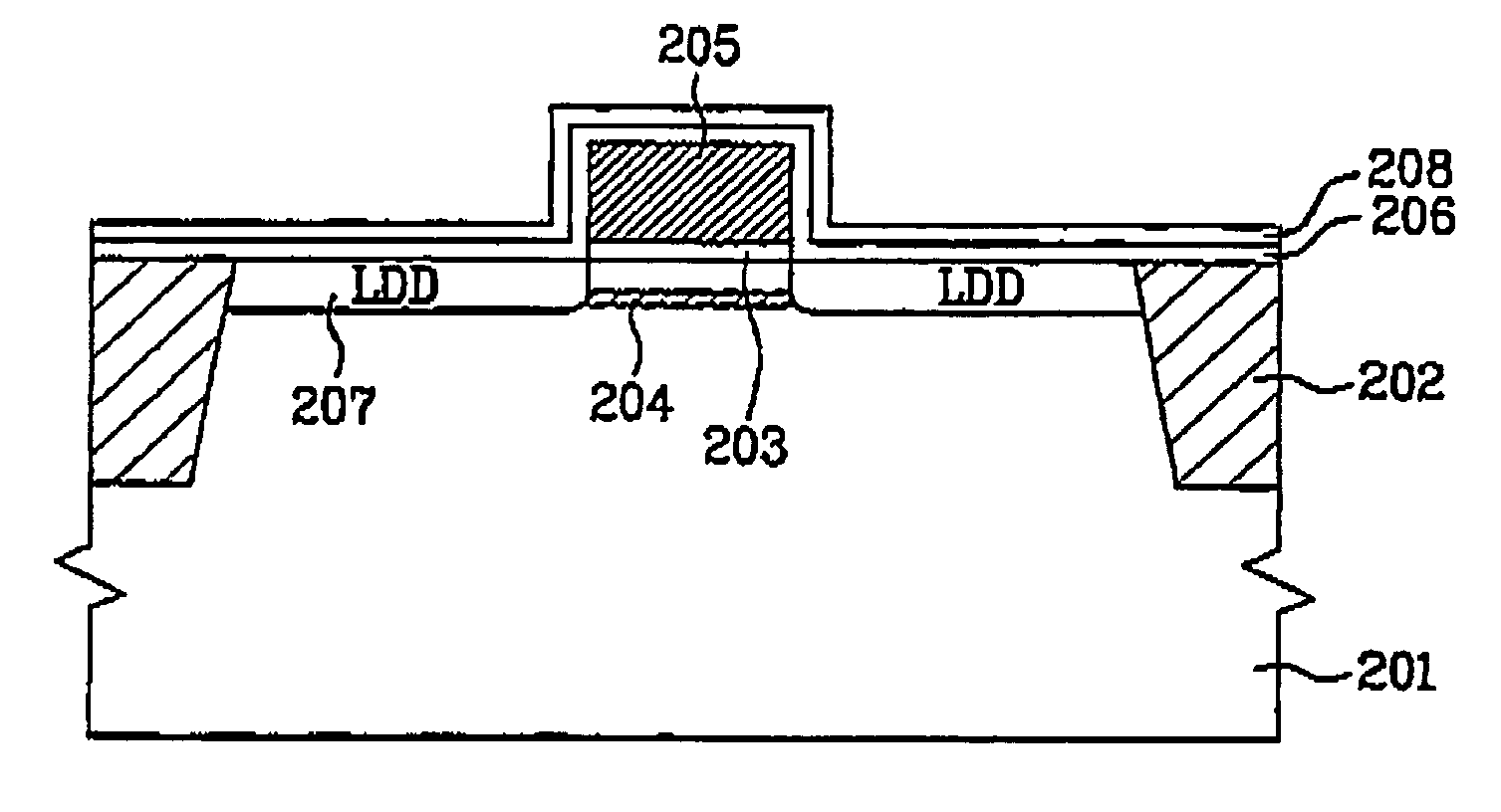
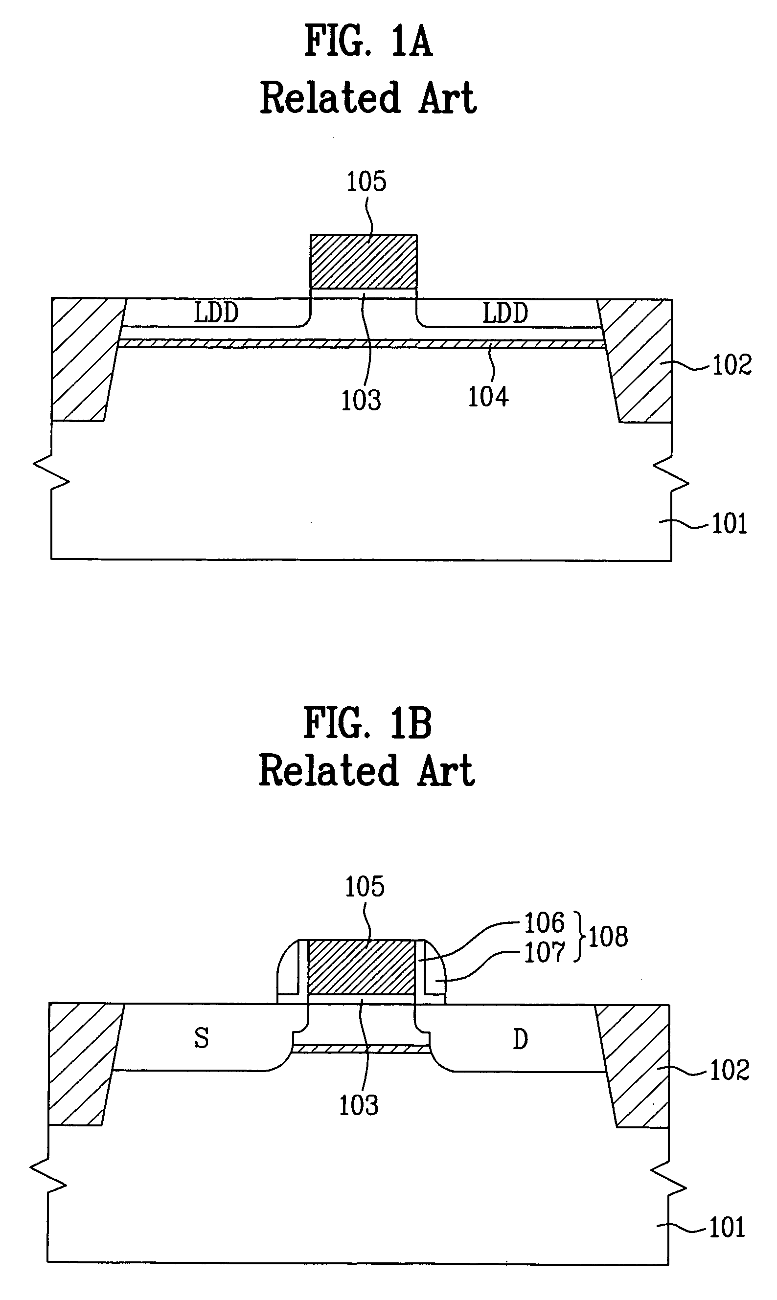
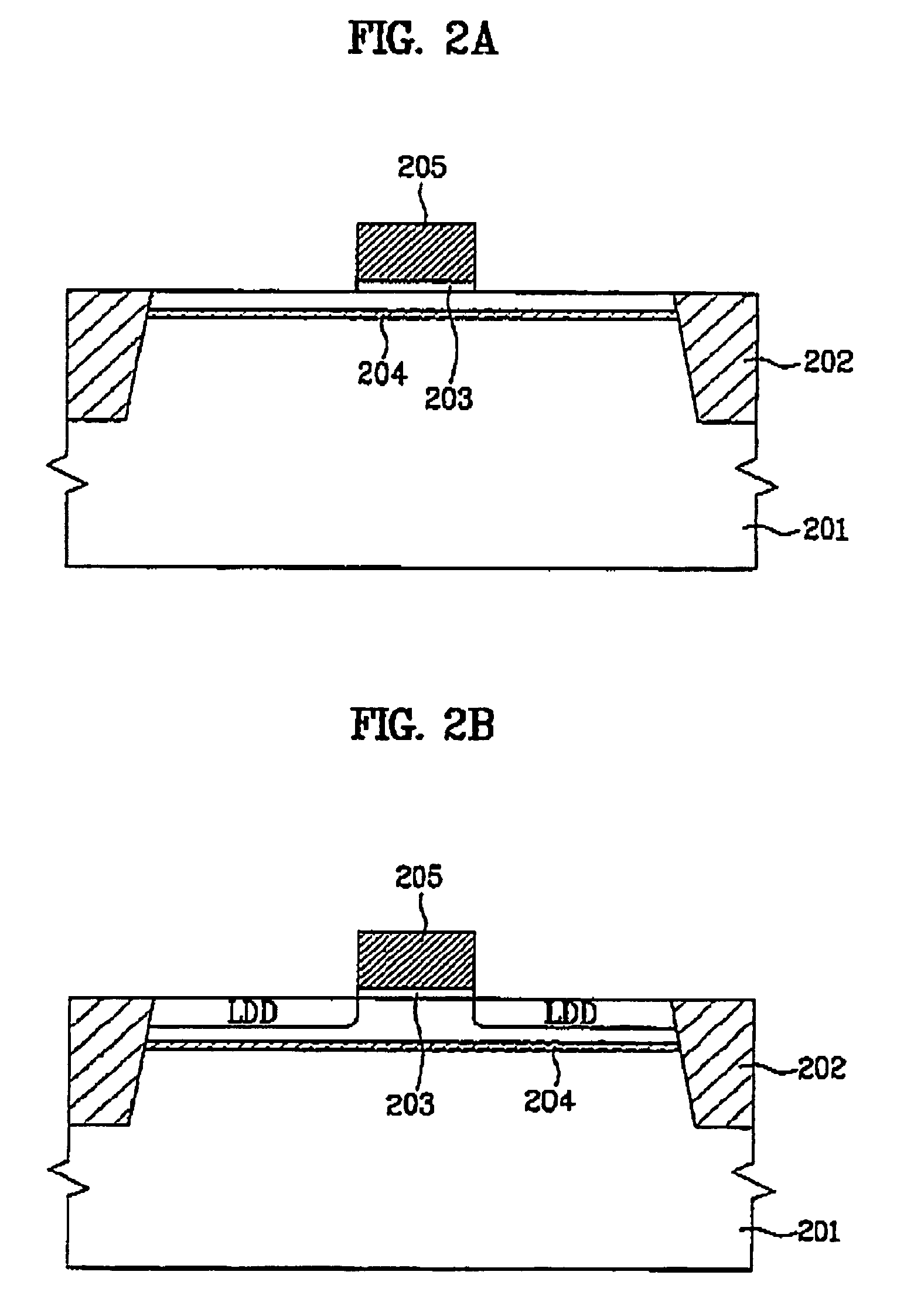
[0035]FIGS. 2A to 2E are cross-sectional diagrams for explaining a method of fabricating a semiconductor device having an LDD structure according to the present invention.

[0036]Referring to FIG. 2A, a device isolation layer 202 is formed on a field area of a semiconductor substrate 201 by STI (shallow trench isolation) or the like to define an active area of the substrate 201. In doing so, a first conductive type (N or P) single crystalline silicon substrate may be used as the semiconductor substrate 201. For convenience of explanation, it is assumed that a first conductive type indicates an N type in the following.

[0037]A gate oxide layer is grown on the active area of the semiconductor substrate 201 by the...


PUM


Abstract

A method of fabricating a semiconductor device is provided, by which leakage current is reduced by minimizing electron or hole density in a source / drain forming a P / N junction with a transistor channel area. The method includes forming a gate insulating layer on a semiconductor substrate, forming a channel ion area in the substrate, forming a gate electrode on the gate insulating layer, forming a sidewall insulating layer on the gate electrode, forming lightly doped regions in the substrate adjacent to the channel ion area and aligned with the gate electrode, forming a spacer insulating layer on the sidewall insulating layer, forming spacers on sidewalls of the gate electrode, and forming heavily doped regions in the substrate aligned with the spacer.

Description

[0001]This application claims the benefit of the Korean Application No. P2003-0101540 filed on Dec. 31, 2003.BACKGROUND OF THE INVENTION[0002]1. Field of the Invention[0003]The present invention relates to a method of fabricating a semiconductor device, by which leakage current is reduced by minimizing electron or hole density in a source / drain forming a P / N junction with a channel area of a transistor.[0004]2. Discussion of the Related Art[0005]Generally, as a semiconductor size is reduced according to a highly increasing degree of semiconductor device integration, a channel length of a semiconductor device is reduced as well. The characteristics of the semiconductor device can be balanced only if the dimensional reduction of the semiconductor is horizontally and vertically made. If such a requirement for the dimensional reduction of the semiconductor device fails to be met, a channel length between source and drain is shortened to result in unfavorable variations of the semiconduc...

Claims


Application Information

Patent Timeline
Patent Type & Authority Patents(United States)
IPC IPC(8): H01L21/336H01L29/10H01L29/78
CPCH01L29/1041H01L29/6656H01L29/6659H01L29/7833H01L21/18
Inventor BANG, KI WAN
Owner COLUMBA TECH INC
Features
  • R&D
  • Intellectual Property
  • Life Sciences
  • Materials
  • Tech Scout
  • Unparalleled Data Quality
  • Higher Quality Content
  • 60% Fewer Hallucinations
Learn More