Supercharge Your Innovation With Domain-Expert AI Agents!

Method for forming dual damascene interconnection in semiconductor device

a technology of damascene and semiconductor devices, which is applied in the direction of semiconductor devices, semiconductor/solid-state device details, electrical apparatus, etc., can solve the problems of deteriorating electrical characteristics and reliability of devices, prone to corrode of lower metal films, etc., and achieve the effect of preventing corrosion of lower metal films

Active Publication Date: 2007-06-19
MARVELL ASIA PTE LTD +1
View PDF5 Cites 3 Cited by
  • Summary
  • Abstract
  • Description
  • Claims
  • Application Information

AI Technical Summary

Benefits of technology

This method effectively prevents corrosion of the lower metal film, enhancing the electrical characteristics and reliability of semiconductor devices by stabilizing the interconnection process.

Problems solved by technology

Accordingly, if the lower metal film is damaged while the etch stop film is removed, there is a problem in that the lower metal film is apt to be corroded when it is exposed to water in the air before and after performing a subsequent process.
If the lower metal film is corroded, electrical characteristics and reliability of devices are deteriorated.

Method used


Image

  • Method for forming dual damascene interconnection in semiconductor device
  • Method for forming dual damascene interconnection in semiconductor device
  • Method for forming dual damascene interconnection in semiconductor device

Examples


Embodiment Construction

[0018]A preferred embodiment of the present invention will now be described in detail with reference to the accompanying drawings. The following embodiments may be modified in various forms, but should not be interpreted to be limited thereto.

[0019]FIGS. 1 to 5 are sectional views illustrating a method for forming a dual damascene interconnection according to the present invention.

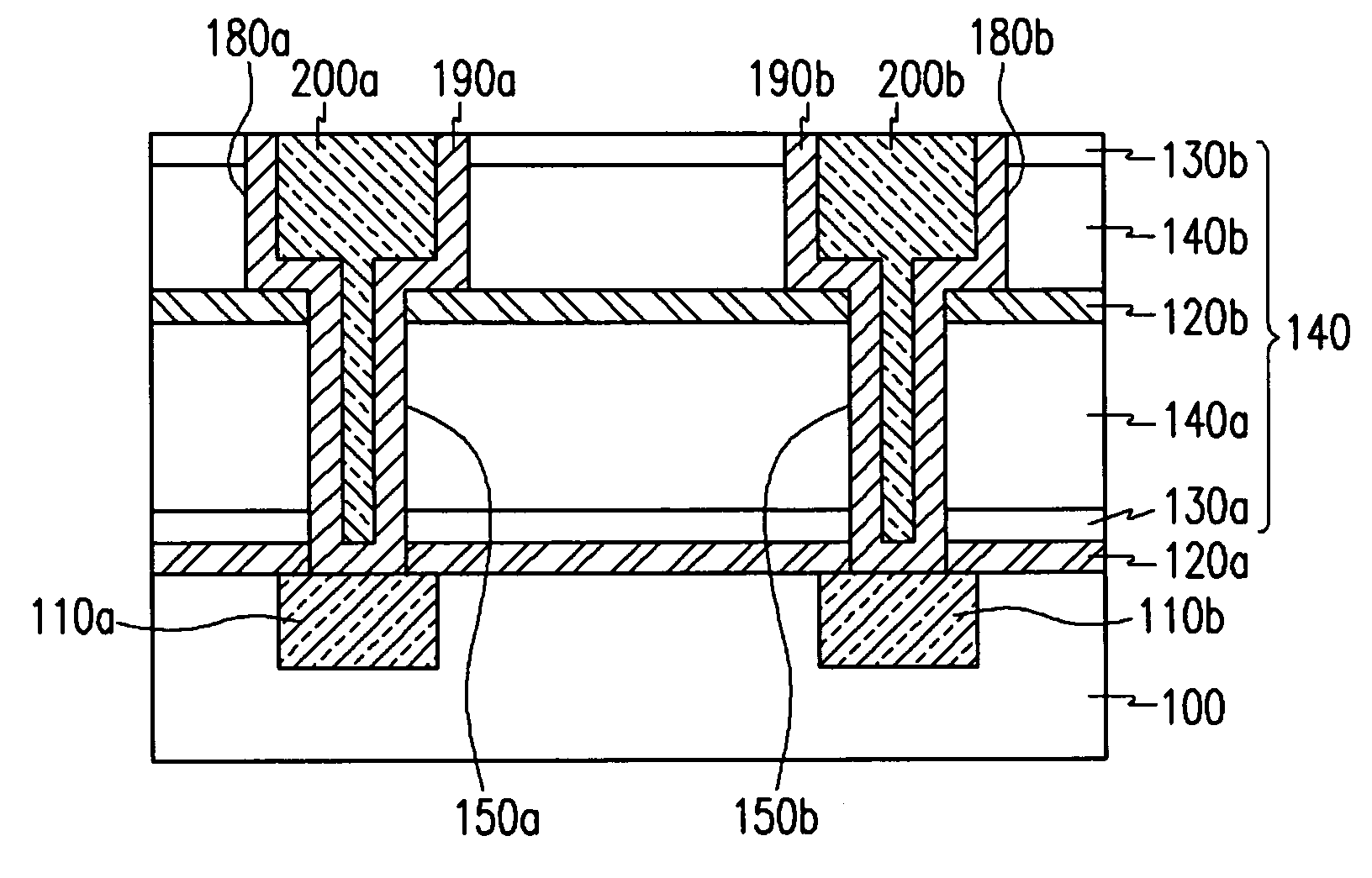
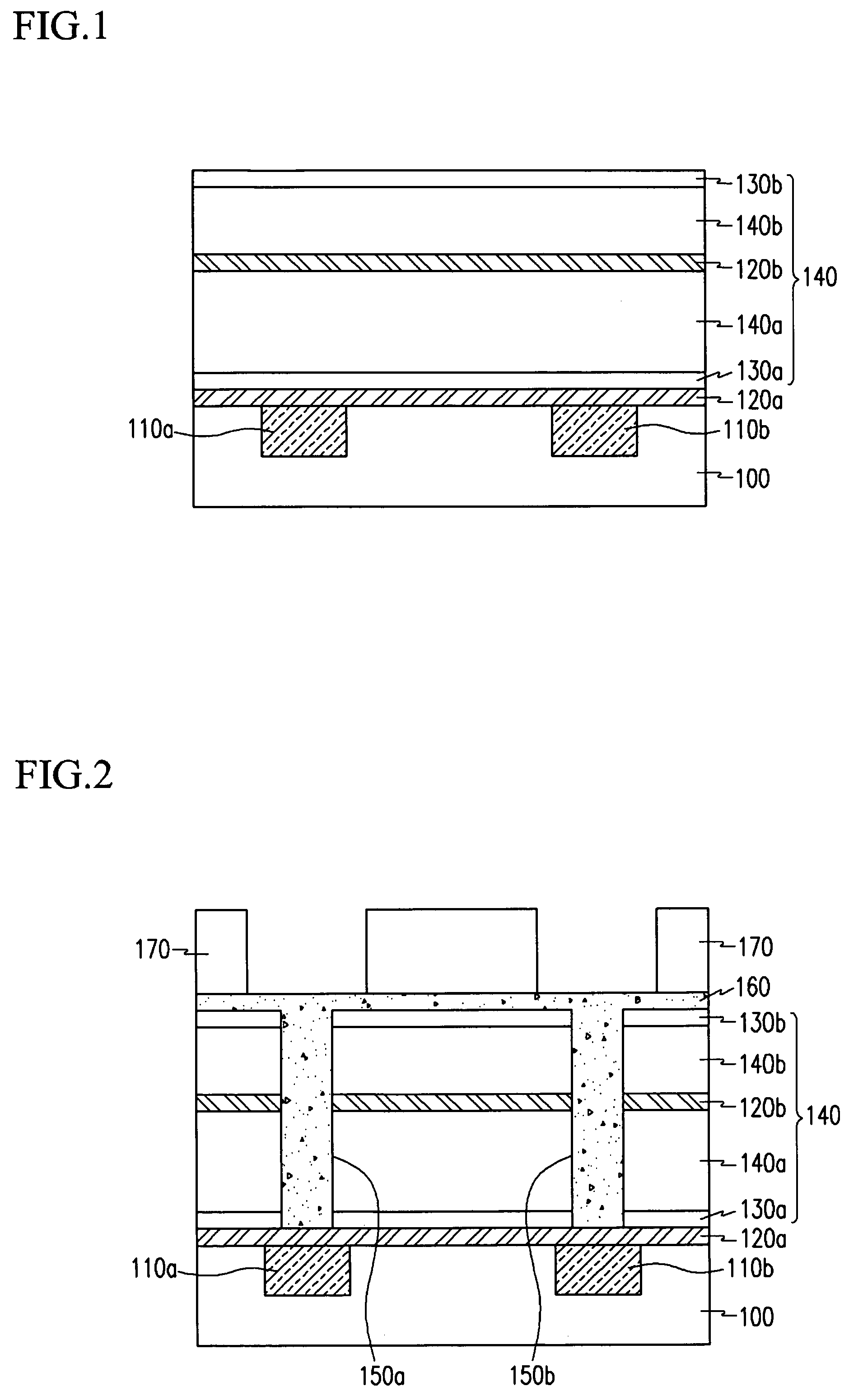
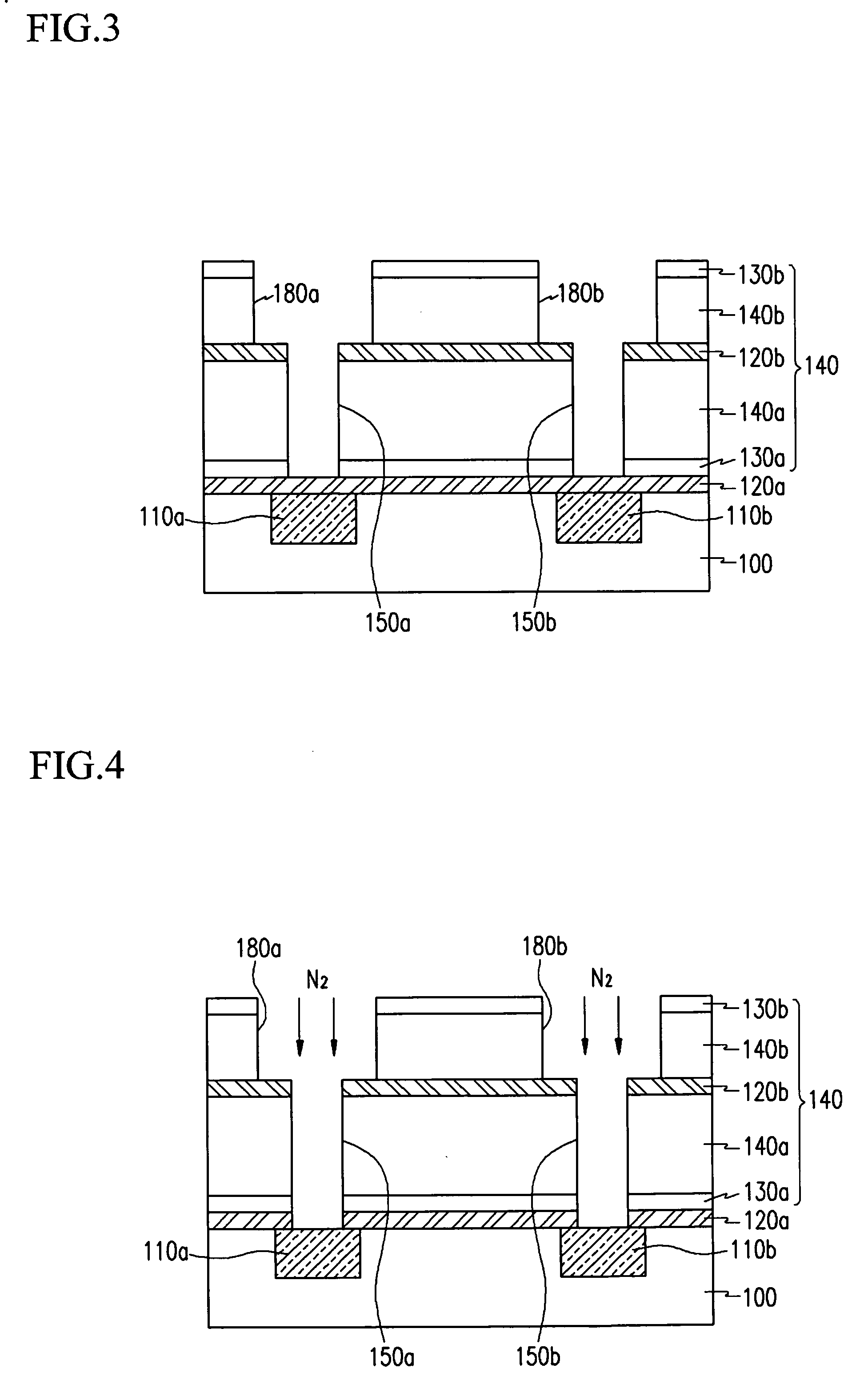
[0020]Referring to FIG. 1, first, a first etch stop film 120a, a first capping film 130a, a first low dielectric insulating film 140a, a second etch stop film 120b, a second low dielectric insulating film 140b, and a second capping film 130b are sequentially formed on an insulating film 100 and lower metal films 110a and 110b disposed within the insulating film 100.

[0021]Although not shown in the figure, the lower metal films 110a and 110b formed with a copper (Cu) film may be connected to other lower metal films or may be directly connected to an impurity region of a semiconductor substrate.

[0022]The firs...


PUM


Abstract

A method for forming a dual damascene interconnection in a semiconductor device, which is capable of preventing a lower metal film from being corroded. The method includes the steps of forming an etch stop film and an intermetal insulating film sequentially on a lower metal film to be interconnected, forming a via hole for exposing a portion of a surface of the etch stop film through the intermetal insulating film, and forming a trench having a width wider than that of the via hole on the intermetal insulating film. The method also includes the steps of exposing the lower metal film by removing the etch stop film by performing an etching process using an etching equipment of a dual plasma source, performing a nitrogen passivation process for the exposed lower metal film, and forming a barrier metal film and an upper metal film sequentially within the trench and the via hole.

Description

BACKGROUND OF THE INVENTION[0001](a) Field of the Invention[0002]The present invention relates to a method for forming an interconnection in a semiconductor device, and more particularly to a method for forming a dual damascene interconnection in a semiconductor device.[0003](b) Description of the Related Art[0004]Recently, as a copper interconnection having an electrical characteristic superior to aluminum (Al) or tungsten (W) has been introduced, a dual damascene process for overcoming a difficulty in dry etching copper is being widely used. In the dual damascene process, a via hole and a trench are first formed, the via hole and the trench are filled with a copper film, and then, a planarization process is performed.[0005]More specifically, an etch stop film and an intermetal insulating film are sequentially formed on a lower metal film, and a via hole is formed using a mask pattern for via hole formation. Next, a trench for exposing the via hole completely is formed using a mask...

Claims


Application Information

Patent Timeline
Patent Type & Authority Patents(United States)
IPC IPC(8): H01L23/48H01L21/302H01L21/44H01L21/461H01L21/4763H01L23/40H01L23/52H01L21/3205H01L21/768
CPCH01L21/76808H01L21/3205
Inventor SHIM, JOON-BUM
Owner MARVELL ASIA PTE LTD
Features
  • R&D
  • Intellectual Property
  • Life Sciences
  • Materials
  • Tech Scout
  • Unparalleled Data Quality
  • Higher Quality Content
  • 60% Fewer Hallucinations
Learn More