

Frame data compensation amount output device, frame data compensation device, frame data display device, and frame data compensation amount output method, frame data compensation method
a technology of frame data and output device, which is applied in the field of matrix-type image display device, can solve the problems of deteriorating the quality level of a video picture to be displayed on the liquid crystal panel, limited input signal, and large circuit scale constituting the device, so as to improve the rate of change in gradation and improve the response rate of liquid crystal
- Summary
- Abstract
- Description
- Claims
- Application Information
AI Technical Summary
Benefits of technology
Problems solved by technology
Method used
Image


Examples
embodiment 1
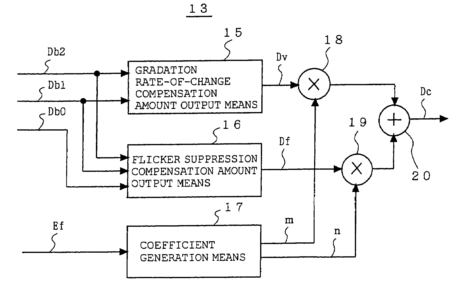
[0044]FIG. 1 is a block diagram showing a constitution of an image display device according to a first preferred embodiment. In the image display device according to this first embodiment, an image signal is inputted to an input terminal 1.
[0045]The image signal having been inputted to the input terminal 1 is received by receiving means 2. Then, the image signal having been received by the receiving means 2 is outputted to a frame data compensation device 3 as frame data Di2 of a digital format (hereinafter, this frame data are also referred to as image data). Herein, the mentioned frame data Di2 stand for data that corresponding to, e.g., number of gradations and chrominance differential signal of a frame that are included in an image signal to be inputted. Further, the mentioned frame data Di2 are the frame data corresponding to a frame targeted (hereinafter, referred to as target frame) to be compensated by the frame data compensation device 3 out of the frames included in the in...
embodiment 2
[0135]A second preferred embodiment is to simplify an internal constitution of the flicker suppression compensation amount output means 16 in the image display device according to the foregoing first embodiment. Hereinafter, such a simplified flicker suppression compensation amount output means 16 is described. Except that there is no input of the decoded data Db0 to the compensation amount output device 13 resulted from the simplification of the flicker suppression compensation amount output means 16, constitution and operation other than those of the flicker suppression compensation amount output means 16 are the same as described in the foregoing first embodiment, so that repeated description thereof is omitted.
[0136]FIG. 14 shows an example, in which the part 21 surrounded by a broken line is simplified in FIG. 6 that shows the mentioned flicker suppression compensation amount output means 16 according to the first embodiment.
[0137]The first decoded data Db2 and the second decod...
embodiment 3
[0146]An image display device according to a third preferred embodiment is to simplify the system constitution of the image display device of the foregoing first and second embodiments.
[0147]Further, the image display device according to this third embodiment makes it possible to suppress flicker interference at a vertical edge occurring in the case where an image signal to be inputted to the mentioned image display device is an interlace signal.
[0148]The flicker interference occurs at a vertical edge of an interlace signal. Thus, in the case where any image signal to be inputted is the interlace signal, it is possible to detect flicker interference by detecting a vertical edge.
[0149]FIG. 16 is a block diagram showing a constitution of an image display device according to the third embodiment. In the image display device according to this third embodiment, an image signal is inputted to an input terminal 1.
[0150]An image signal having been inputted to the input terminal 1 is receive...
PUM
 Abstract
Description
Claims
Application Information