Check patentability & draft patents in minutes with Patsnap Eureka AI!

Method for manufacturing a flexible panel for a flat panel display

a flat panel display and flexible technology, applied in the manufacture of electrode systems, discharge tubes luminescent screens, instruments, etc., can solve the problems of low yield rate, difficult re-design or modification, and inferior device characteristics and film quality of plastic substrates to those made on glass substrates

Inactive Publication Date: 2007-11-20
IND TECH RES INST
View PDF6 Cites 22 Cited by
  • Summary
  • Abstract
  • Description
  • Claims
  • Application Information

AI Technical Summary

Benefits of technology

This method enables the production of flexible panels with improved adhesion and film quality, overcoming the limitations of plastic substrates by leveraging the superior properties of glass substrates, particularly in organic thin film transistors, and allowing for mass production of large-size panels with enhanced moisture resistance and reduced stress.

Problems solved by technology

However, the device characteristics and film quality made on the plastic substrate are inferior to those made on the glass substrate because the plastic substrate can not resist to the high-processing temperature, around 300 to 400 degrees C. Although Sharp Co. has developed a plastic substrate that is capable of withstanding up to approx. 220 degrees C., there is still a need to re-design or modify the conventional FPD process due to the plasticity and flexibility of the plastic substrate.
Besides, such technique is quite difficult and low yield rate.
As for organic thin film transistors (OTFT), the plastic substrate especially needs severe treatments because the organic materials are extremely sensitive to moisture.
Although the plastic substrate is lightweight, thin, and flexible, it has too low a Tg (glass transition temperature) point to withstand high temperature processing, that influences the characteristics of the devices.
In addition to that, the problems during the fabrication of thin film devices on the plastic substrate, such as the stress, the static electricity, and the thermal expansion are not easy to be overcome.

Method used


Image

  • Method for manufacturing a flexible panel for a flat panel display
  • Method for manufacturing a flexible panel for a flat panel display
  • Method for manufacturing a flexible panel for a flat panel display

Examples


example 1

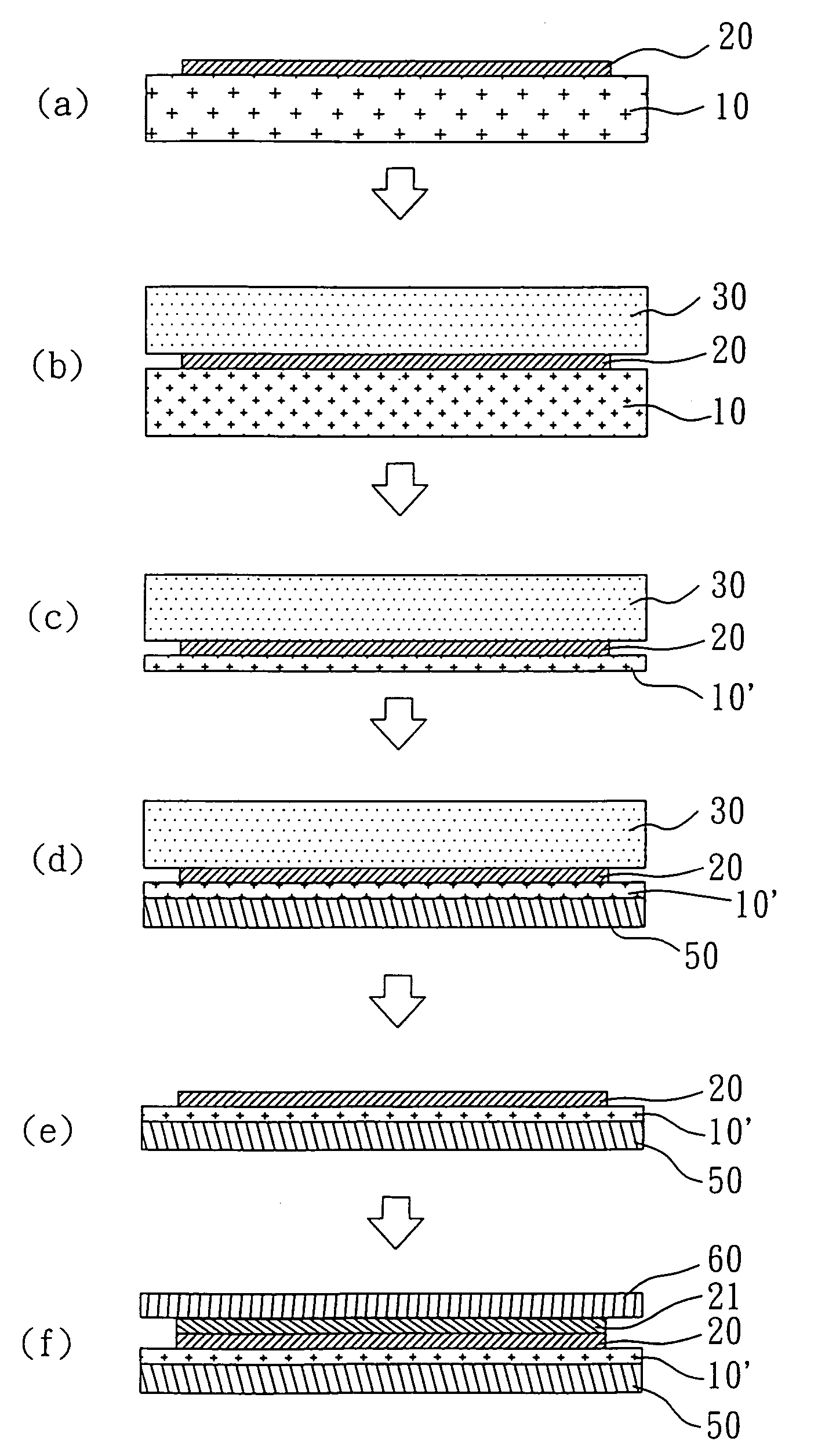
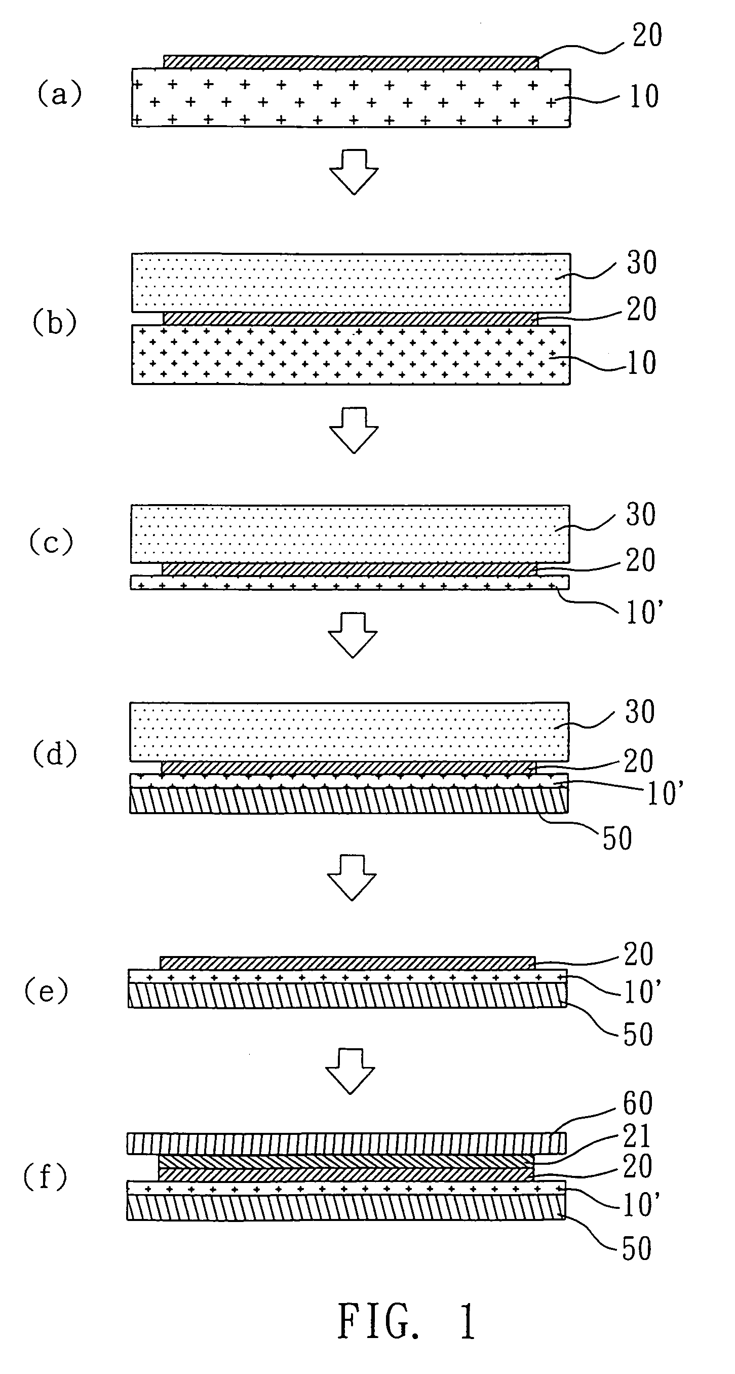
[0022]With reference to FIG. 1, there is shown the flow diagram of the first example of the present invention. The method for manufacturing a flexible panel of the present invention includes the following steps. First, a first substrate 10 is provided having a plurality of functional switches or conducting lines 20 formed thereon. The functional switches may be thin film transistors. Next, the second substrate 30 is bonded on the functional switches or conducting lines 20. Afterwards, the first substrate 10 is thinned to a predetermined thickness. The flexible third substrate 50 is subsequently adhered on the thinned first substrate 10′ so that the thinned first substrate 10′ is sandwiched between the second substrate 30 and the flexible third substrate 50. Finally, the second substrate 30 is removed.

[0023]It is optional to form a plurality of light valves, light-emitters, or conducting layers 21 on the functional switches or conducting lines 20 and then the flexible fourth substrat...

example 2

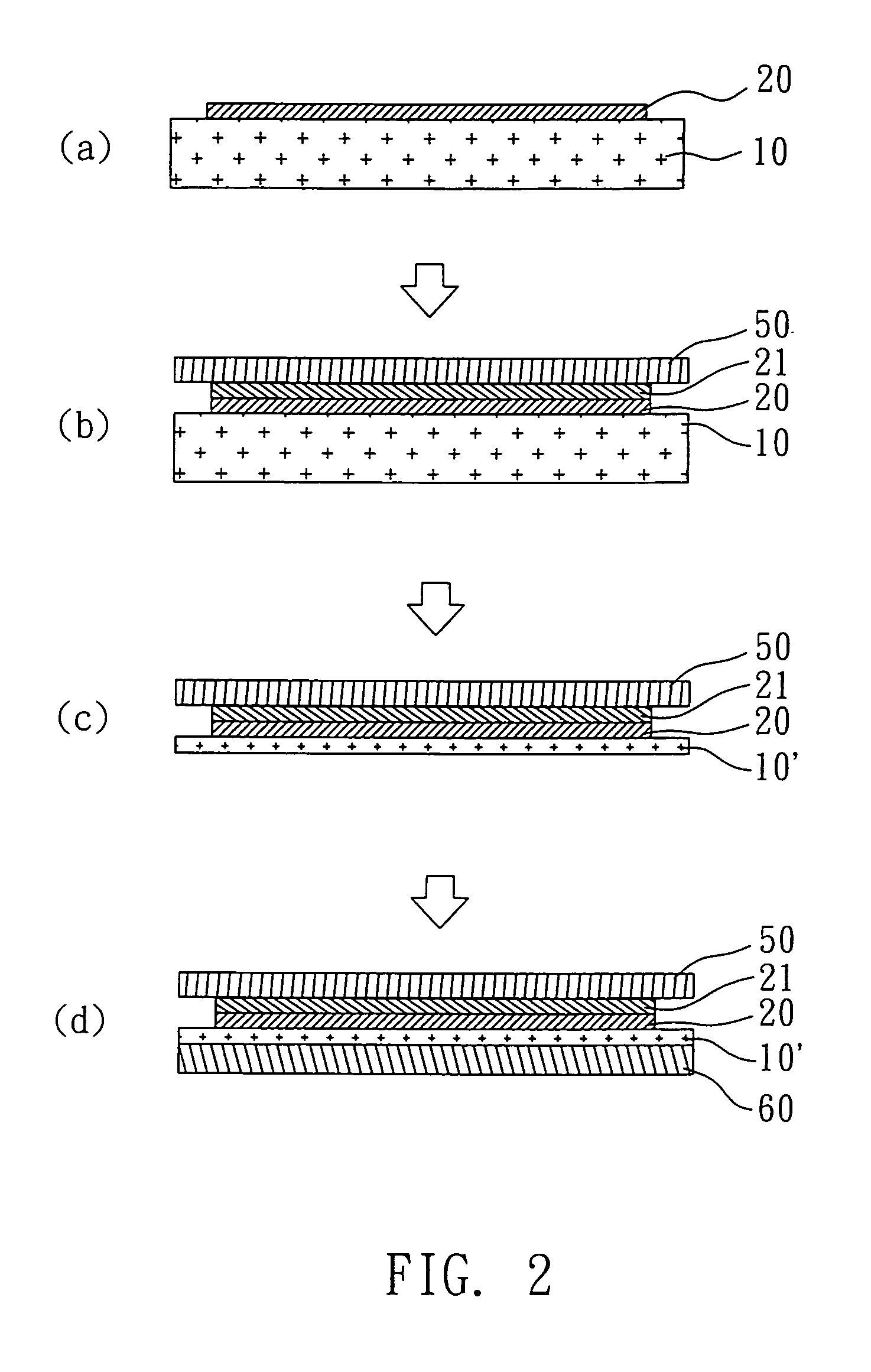
[0024]With reference to FIG. 2, there is shown the flow diagram of the second example of the present invention. The method for manufacturing a flexible panel of the present example will be illustrated as follows. The first substrate 10 having a plurality of functional switches or conducting lines 20 formed thereon is provided first. Afterwards, a plurality of light valves, light-emitters, or conducting layers 21 is formed on the functional switches or conducting lines 20, and the flexible third substrate 50 is adhered on the light valves, light-emitters, or conducting layers 21. As a result, the functional switches or conducting lines 20 and the light valves, light-emitters, or conducting layers 21 are sandwiched between the first substrate 10 and the third substrate 50. The first substrate 10 is then thinned to a predetermined thickness and forms the thinned first substrate 10′. Finally, the flexible fourth substrate 60 is adhered on the thinned first substrate 10′ so that the func...

example 3

[0025]With reference to FIG. 3, there is shown the flow diagram of the third example of the present invention. The method for manufacturing a flexible panel of the present example will be illustrated as follows. The first substrate 10 having a plurality of functional switches or conducting lines 20 formed thereon is provided first. The functional switches are thin film transistors in the present example. Next, the second substrate 30 is bonded on the functional switches or conducting lines 20, and then the first substrate 10 is thinned to a predetermined thickness to form the thinned first substrate 10′. Afterwards, the fifth substrate 70 is adhered on the thinned first substrate 10′ and subsequently the second substrate 30 is removed. Next, a plurality of light valves, light-emitters, or conducting layers 21 is formed on the functional switches or conducting lines 20, and then the fifth substrate 70 is removed. Finally, the surface of the whole substrate is coated with a flexible p...


PUM

PropertyMeasurementUnit
thicknessaaaaaaaaaa
thicknessaaaaaaaaaa
flexibleaaaaaaaaaa

Abstract

A method for manufacturing a flexible panel is disclosed, which has the following steps. First, a first substrate having a plurality of functional switches or conducting lines thereon is provided. Then, a second substrate is bonded on the functional switches or conducting lines, and the first substrate is thinned to a predetermined thickness subsequently. Afterwards, a flexible third substrate is adhered on the first substrate, wherein the first substrate is sandwiched between the second substrate and the third substrate. Finally, the second substrate is removed.

Description

[0001]This application is a continuation of nonprovisional application Ser. No. 10 / 695,810, filed Oct. 30, 2003 now U.S. Pat. No. 7,147,531.BACKGROUND OF THE INVENTION[0002]1. Field of the Invention[0003]The present invention relates to a method for manufacturing a flexible panel and, more particularly, to a method for manufacturing a flexible panel for a flat panel display.[0004]2. Description of Related Art[0005]As one trend in flat panel display technologies is increasing the display areas, a parallel trend is the developments in technical innovations of minimizing weight and thickness. A key one of those developments is to replace the glass substrate with a plastic substrate. However, the device characteristics and film quality made on the plastic substrate are inferior to those made on the glass substrate because the plastic substrate can not resist to the high-processing temperature, around 300 to 400 degrees C. Although Sharp Co. has developed a plastic substrate that is capa...

Claims


Application Information

Patent Timeline
Patent Type & Authority Patents(United States)
IPC IPC(8): H01J9/26G02F1/1333H01J9/24
CPCG02F1/133305H01J9/241H01J2217/492G02F2001/13613G02F1/13613
Inventor CHANG, JUNG-FANGCHANG, CHICH-SHANGCHEN, CHI-LIN
Owner IND TECH RES INST
Features
  • R&D
  • Intellectual Property
  • Life Sciences
  • Materials
  • Tech Scout
  • Unparalleled Data Quality
  • Higher Quality Content
  • 60% Fewer Hallucinations
Learn More