Supercharge Your Innovation With Domain-Expert AI Agents!

Semiconductor memory device capable of setting a negative threshold voltage

a memory device and negative threshold technology, applied in the field of semiconductor memory devices, can solve the problems of slow program speed, slow write speed, complicated manufacturing process,

Active Publication Date: 2008-04-29
KIOXIA CORP
View PDF10 Cites 30 Cited by
  • Summary
  • Abstract
  • Description
  • Claims
  • Application Information

AI Technical Summary

Benefits of technology

This approach enables high-speed writing by widening the threshold voltage range, reducing the number of program and verify operations, and stabilizing the power supply, while simplifying the manufacturing process by avoiding the need for high withstand voltage transistors in a p-well structure.

Problems solved by technology

This causes a problem: the speed of the program becomes slower.
In this control, too, a program operation and a program verify operation must be repeated as described above, which causes a problem: the write speed becomes slower.
This causes a problem: the manufacturing process becomes complicated.
However, this technique has been applied to the test mode of memory cells, and not to the normal operation mode.
In addition, when the internal power supply circuit applies a bias voltage to the source and well, large currents flow from a large number (16 k to 32 k) of bit lines into the internal power supply circuit, which causes a problem: the internal power supply circuit is unstable.

Method used


Image

  • Semiconductor memory device capable of setting a negative threshold voltage
  • Semiconductor memory device capable of setting a negative threshold voltage
  • Semiconductor memory device capable of setting a negative threshold voltage

Examples


first embodiment

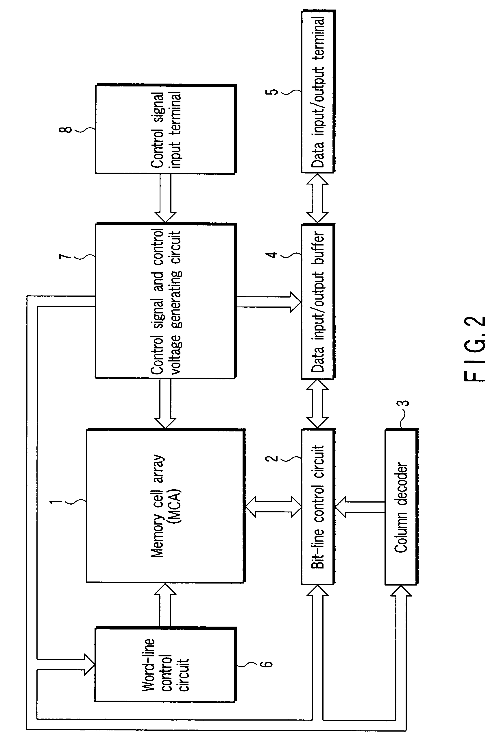
[0032]FIG. 2 shows the configuration of a semiconductor memory device according to a first embodiment of the present invention, more specifically, the configuration of, for example, a NAND flash memory which stores 4-valued (2-bit) data.

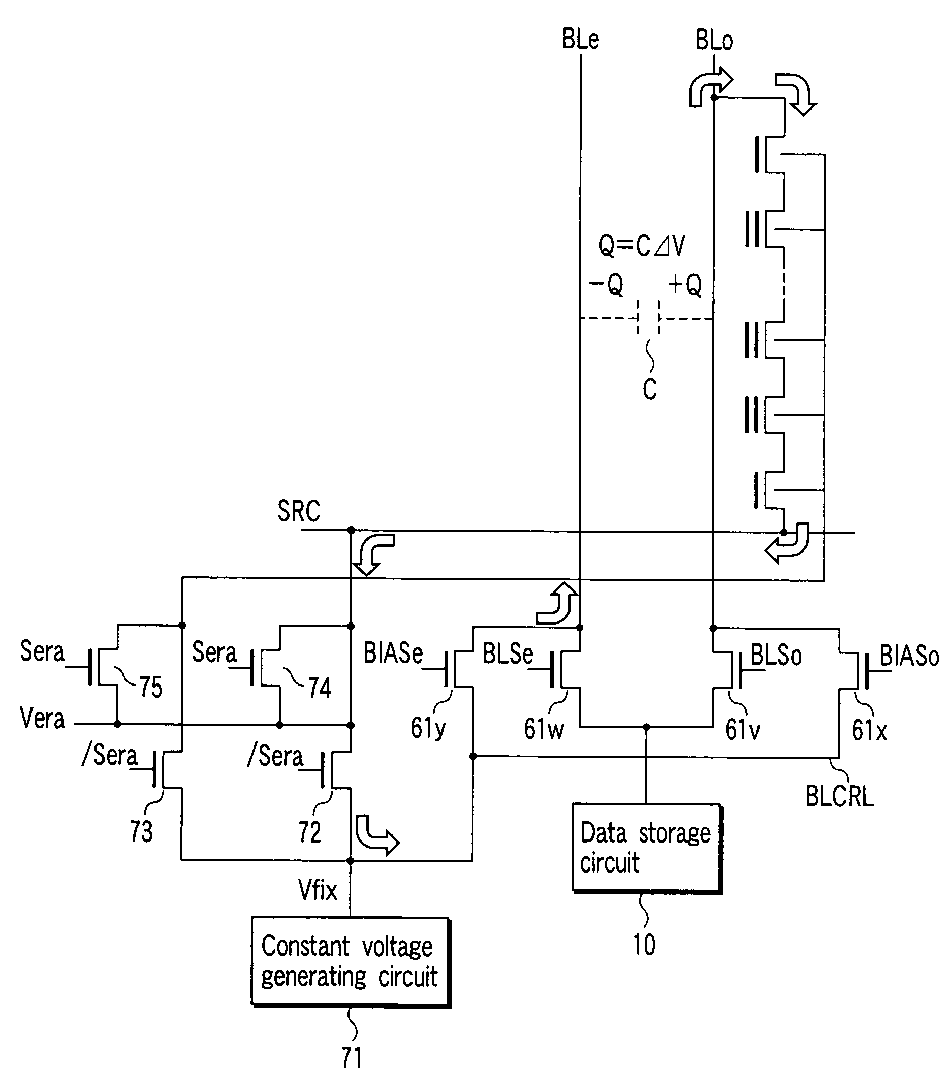
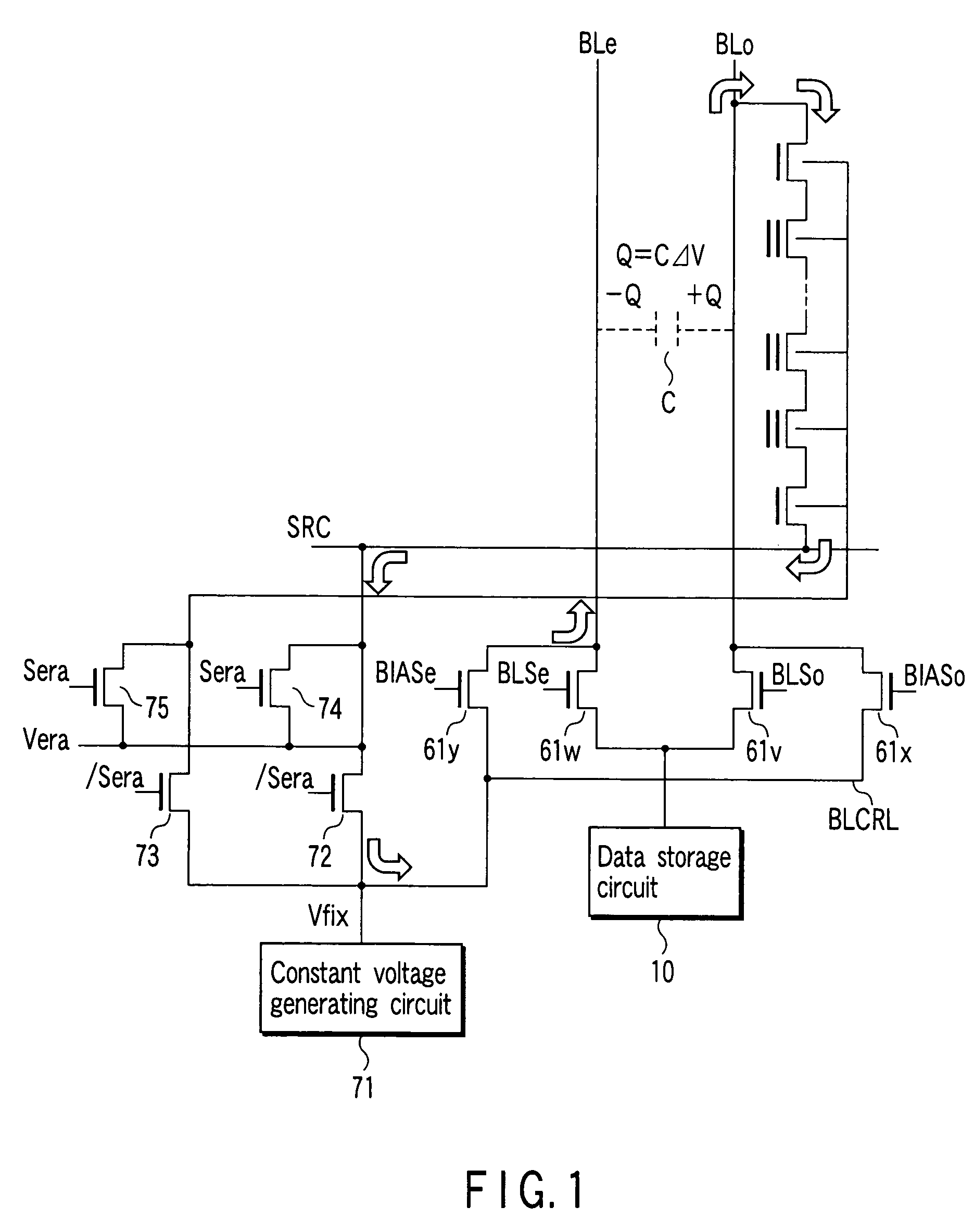
[0033]A memory cell array 1 includes a plurality of bit lines, a plurality of word lines, and a common source line. In the memory cell array 1, memory cells each of which is composed of, for example, an EEPROM cell and enables data to be rewritten electrically are arranged in a matrix. A bit control circuit 2 for controlling the bit lines and a word-line control circuit 6 are connected to the memory cell array 1.

[0034]The bit-line control circuit 2 reads data in a memory cell in the memory cell array via a bit line, detects the state of a memory cell in the memory cell array 1 via a bit line, or writes data into a memory cell by applying a write control voltage to the memory cell in the memory cell array 1 via a bit line. A column decoder 3 and a dat...

second embodiment

[0125]In the first embodiment, the operation of setting the threshold voltage of an erased cell at −1.6 V is carried out during an erase sequence. However, as shown in FIG. 11, the operation may be carried out in the first page program or the second page program.

[0126]According to a second embodiment of the present invention, the erase operation can be made faster, although the program operation gets a little slower.

third embodiment

[0127]In a positive read and a program verify operation and a negative read and a program verify operation in the first and second embodiments, when the voltage applied to the well of the selected cell, the source line, the unselected bit lines, and the select gates of the unselected blocks is negative, it is changed to Vfix (e.g., 1.6 V). When the voltage is positive, it is changed to Vss. The invention is not limited to this. For instance, when the voltage is positive, the voltage applied to the well of the selected cell, the source line, the unselected bit lines, and the select gates of the unselected blocks may be changed to Vfix as when the voltage is negative.

[0128]According to a third embodiment of the present invention, it is not necessary to change the read operation between a positive read and a negative read. Therefore, a positive read operation and a negative read operation can be carried out under the same conditions.

[0129]Furthermore, in the first and second embodiment...


PUM


Abstract

In a memory cell array, a plurality of memory cells connected to word lines and bit lines are arranged in a matrix. A control circuit controls the potentials of the word lines and bit lines. The control circuit, when reading data from the memory cell connected to a first one of the bit lines, supplies a first voltage to a second bit line provided next to the first bit line and to a source line of the memory cell array.

Description

CROSS-REFERENCE TO RELATED APPLICATIONS[0001]This application is based upon and claims the benefit of priority from prior Japanese Patent Application No. 2004-364902, filed Dec. 16, 2004, the entire contents of which are incorporated herein by reference.BACKGROUND OF THE INVENTION[0002]1. Field of the Invention[0003]This invention relates to a semiconductor memory device capable of storing binary or more-valued data in, for example, a single memory.[0004]2. Description of the Related Art[0005]In a NAND flash memory, all of or half of a plurality of memory cells arranged in the row direction are connected via bit lines to corresponding latch circuits, respectively. Each latch circuit holds data in writing or reading data. Data is written or read all at once into or from all of or half of the cells arranged in the row direction (for example, refer to Jpn. Pat. Appln. KOKAI Publication No. 2004-192789).[0006]In addition, data is erased in, for example, blocks. The threshold voltage of ...

Claims


Application Information

Patent Timeline
Patent Type & Authority Patents(United States)
IPC IPC(8): G11C16/04
CPCG11C11/5628G11C16/0483G11C16/12G11C16/3454G11C16/30G11C16/04G11C15/04
Inventor SHIBATA, NOBORU
Owner KIOXIA CORP
Features
  • R&D
  • Intellectual Property
  • Life Sciences
  • Materials
  • Tech Scout
  • Unparalleled Data Quality
  • Higher Quality Content
  • 60% Fewer Hallucinations
Learn More