Supercharge Your Innovation With Domain-Expert AI Agents!

Wafer level packaging cap and fabrication method thereof

a technology of packaging cap and wafer, which is applied in the direction of gaseous heating fuel, household stoves or ranges, lighting and heating apparatus, etc., can solve the problems of high temperature, inconvenient processing time, and difficult to reduce the thickness of the cap substrate to 300 m or less, and achieves simple structure and easy manufacturing method

Active Publication Date: 2009-05-05
SAMSUNG ELECTRONICS CO LTD
View PDF9 Cites 7 Cited by
  • Summary
  • Abstract
  • Description
  • Claims
  • Application Information

AI Technical Summary

Benefits of technology

[0022]An aspect of the present invention is to address the above problems and / or disadvantages of the related art and to provide at least the advantages described below. Accordingly, an aspect of the present invention is to provide a wafer level packaging cap and a fabrication method thereof, which has a simple structure and an easy manufacturing method.

Problems solved by technology

Generally, minute structures manufactured in a chip unit such as an RF filter, a communication-use RF switch and an RF MEMS, and particular function-performing devices such as an actuator, are vulnerable to water, other particles and high temperature, accordingly requiring packaging.
However, the packaging cap manufactured through the above-described process has the following problems.
The connection holes of the wafer need to penetrate the wafer, inconveniently requiring a long processing time.
That is, common silicon (Si) wafer which is used as the cap substrate has a difficulty in lowering the thickness of the cap substrate to 300 μm or less, due to the inconvenience in processing of the Si.
Accordingly, it is hard to save unit costs.
The connection hole which penetrates the wafer requires a longer time for plating metal materials in deep connection holes and thus increases the entire costs.
The connection holes formed on the cap substrate are directly plated with the metal materials, so the metal materials fail to be firmly attached to the holes, dropping electric stability.

Method used


Image

  • Wafer level packaging cap and fabrication method thereof
  • Wafer level packaging cap and fabrication method thereof
  • Wafer level packaging cap and fabrication method thereof

Examples


Embodiment Construction

[0055]Hereinafter, exemplary embodiments of the present invention will be described in detail with reference to the accompanying drawing figures.

[0056]In the following description, the same drawing reference numerals are used for the same elements even in different drawings. The matters defined in the description such as a detailed construction and elements are provided simply to assist in a comprehensive understanding of the invention. Thus, it is apparent that the present invention can be carried out without those defined matters. Also, well-known functions or constructions are not described in detail since they are not necessary for understanding the invention.

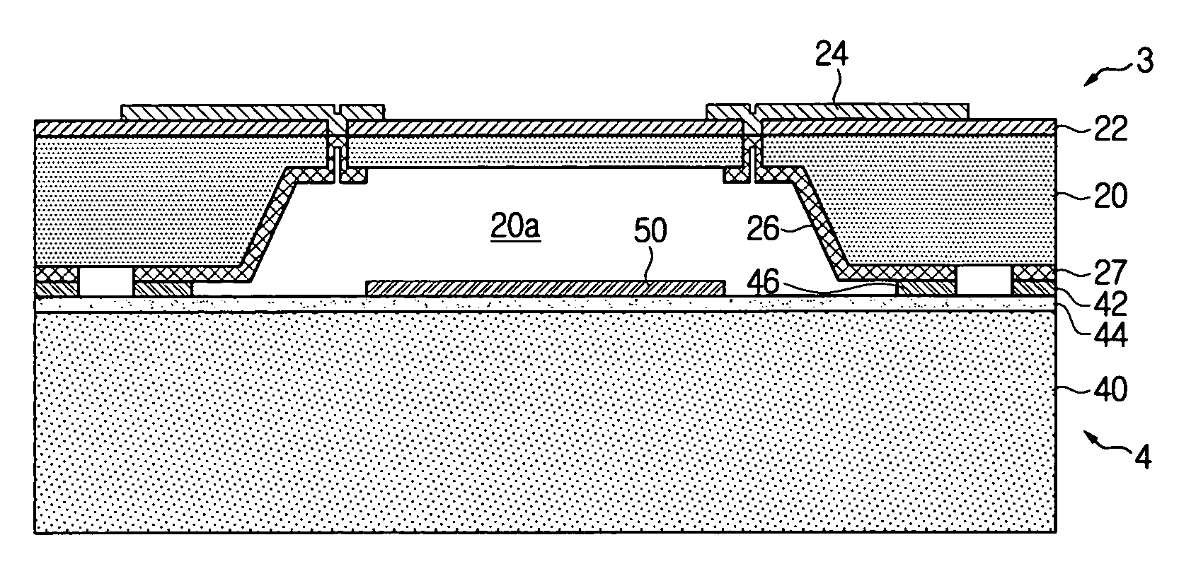
[0057]Referring to FIGS. 2A and 2B, a wafer level packaging cap 3 according to an exemplary embodiment of the present invention is used to cover an upper part of a device wafer 4 having a device 50 on an upper surface thereof. The packaging cap 3 includes a cap substrate 20 having a cavity 20a on a lower part thereof, an in...


PUM


Abstract

A fabrication method of a wafer level packaging cap for covering a device wafer provided with a device thereon, includes forming an insulating layer on a wafer; removing a predetermined part of the insulating layer and exposing an upper surface of the wafer; forming a cap pad extending from an upper surface and the exposed surface of the wafer; forming a cavity on a lower surface of the wafer corresponding to the cap pad; etching a bottom surface of the cavity and exposing the cap pad which is connected to the wafer through the cavity; and forming metal lines extending from the lower surface of the wafer and the cavity, to electrically connect the cap pad which is exposed through the cavity.

Description

CROSS-REFERENCE TO RELATED APPLICATIONS[0001]This application claims priority under 35 U.S.C. § 119(a) of Korean Patent Application No. 10-2006-0004560, filed Jan. 16, 2006, in the Korean Intellectual Property Office, the entire contents of which are incorporated herein by reference.BACKGROUND OF THE INVENTION[0002]1. Field of the Invention[0003]The present invention relates to a wafer level packaging method. More particularly, the present invention relates to a wafer level packaging cap used for the packaging method, and a fabrication method thereof.[0004]2. Description of the Related Art[0005]Generally, minute structures manufactured in a chip unit such as an RF filter, a communication-use RF switch and an RF MEMS, and particular function-performing devices such as an actuator, are vulnerable to water, other particles and high temperature, accordingly requiring packaging.[0006]The packaging is performed by covering and sealing up an upper surface of a device wafer formed with the ...

Claims


Application Information

Patent Timeline
Patent Type & Authority Patents(United States)
IPC IPC(8): H01L23/12H01L23/10
CPCB81C1/00301H01L23/04B81B2207/095B81C2203/0118H01L2924/01079H01L2924/16235F24C3/126F24C3/14
Inventor KIM, YONG-SUNGKIM, WOON-BAEJUNG, KYU-DONGLEE, CHANG-SEUNG
Owner SAMSUNG ELECTRONICS CO LTD
Features
  • R&D
  • Intellectual Property
  • Life Sciences
  • Materials
  • Tech Scout
  • Unparalleled Data Quality
  • Higher Quality Content
  • 60% Fewer Hallucinations
Learn More