Supercharge Your Innovation With Domain-Expert AI Agents!

Memory device and method of manufacturing the same

a memory device and memory technology, applied in the field of memory devices, can solve the problems of difficult scale-down methods, conventional methods of increasing the integration of semiconductor memory devices by decreasing the size of unit members of semiconductor memory devices, etc., and achieve the effect of improving integration

Inactive Publication Date: 2009-05-19
SAMSUNG ELECTRONICS CO LTD
View PDF7 Cites 7 Cited by
  • Summary
  • Abstract
  • Description
  • Claims
  • Application Information

AI Technical Summary

Benefits of technology

This approach allows for increased integration of memory devices, enabling storage of more logic levels per unit cell without downsizing individual components, thereby improving memory capacity without the limitations of traditional scaling methods.

Problems solved by technology

However, conventional methods to increase integration of semiconductor memory devices by decreasing the size of unit members of the semiconductor memory devices (hereinafter “scale-down methods”) have been difficult due to technical limits of performing a photolithographical process and degradation of the unit members generated by a short channel effect.
Although methods of increasing integration outside of decreasing the size of the unit members have been studied, integration of the semiconductor memory devices has not been sufficient and remains an essential subject for development.

Method used


Image

  • Memory device and method of manufacturing the same
  • Memory device and method of manufacturing the same
  • Memory device and method of manufacturing the same

Examples


Embodiment Construction

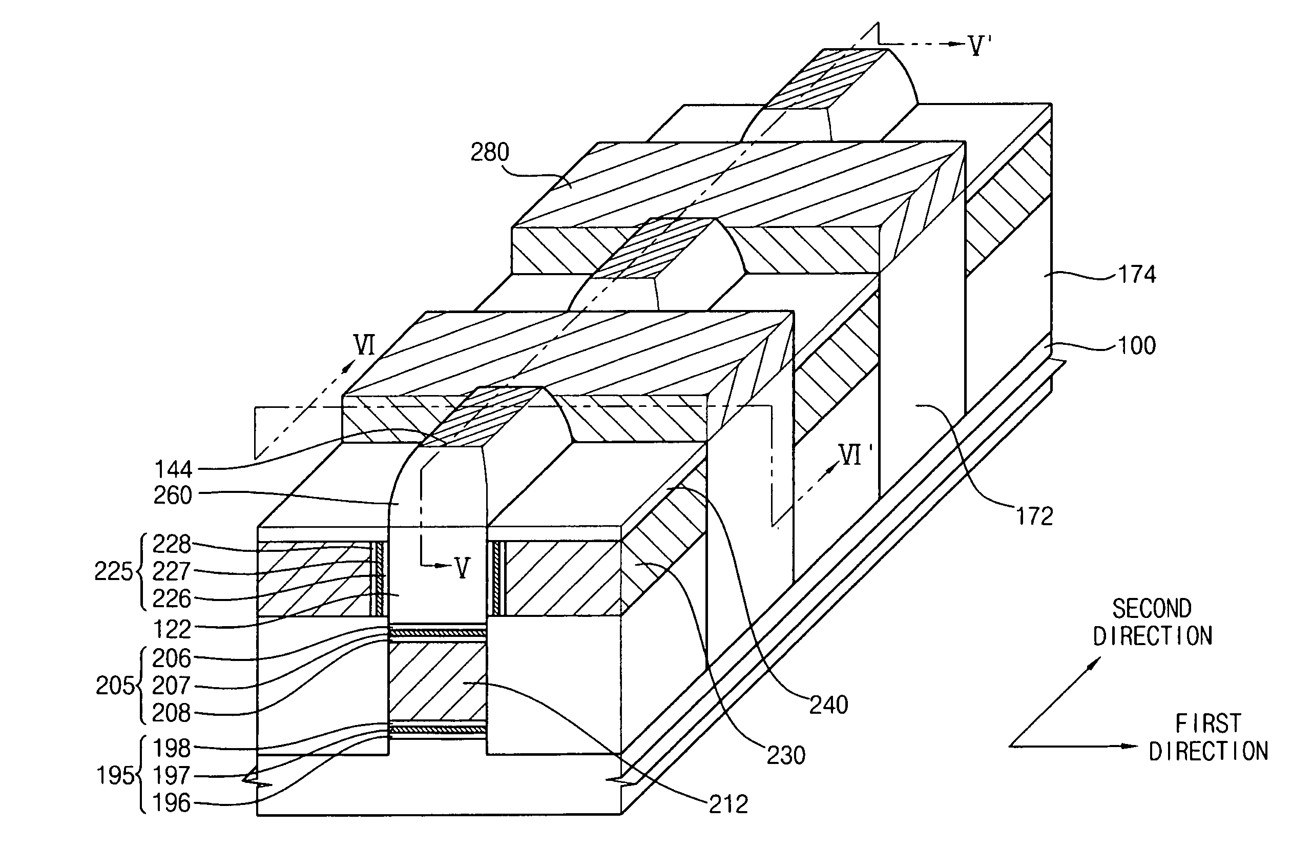
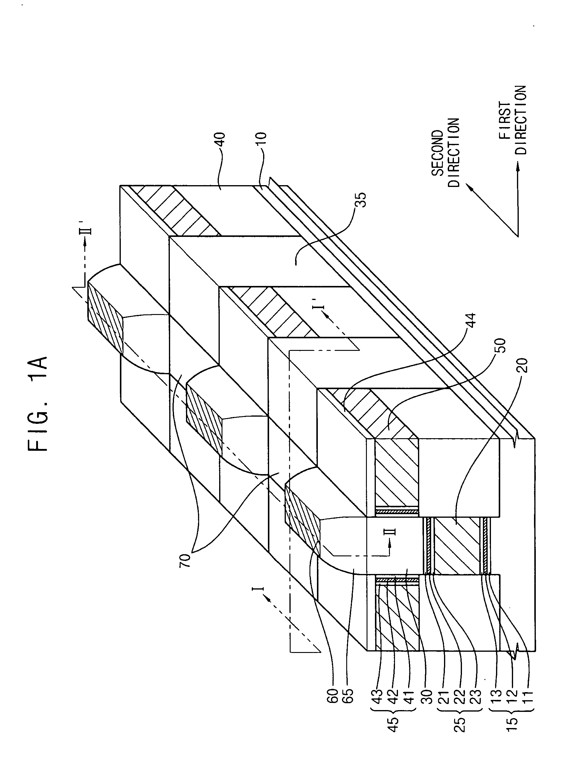
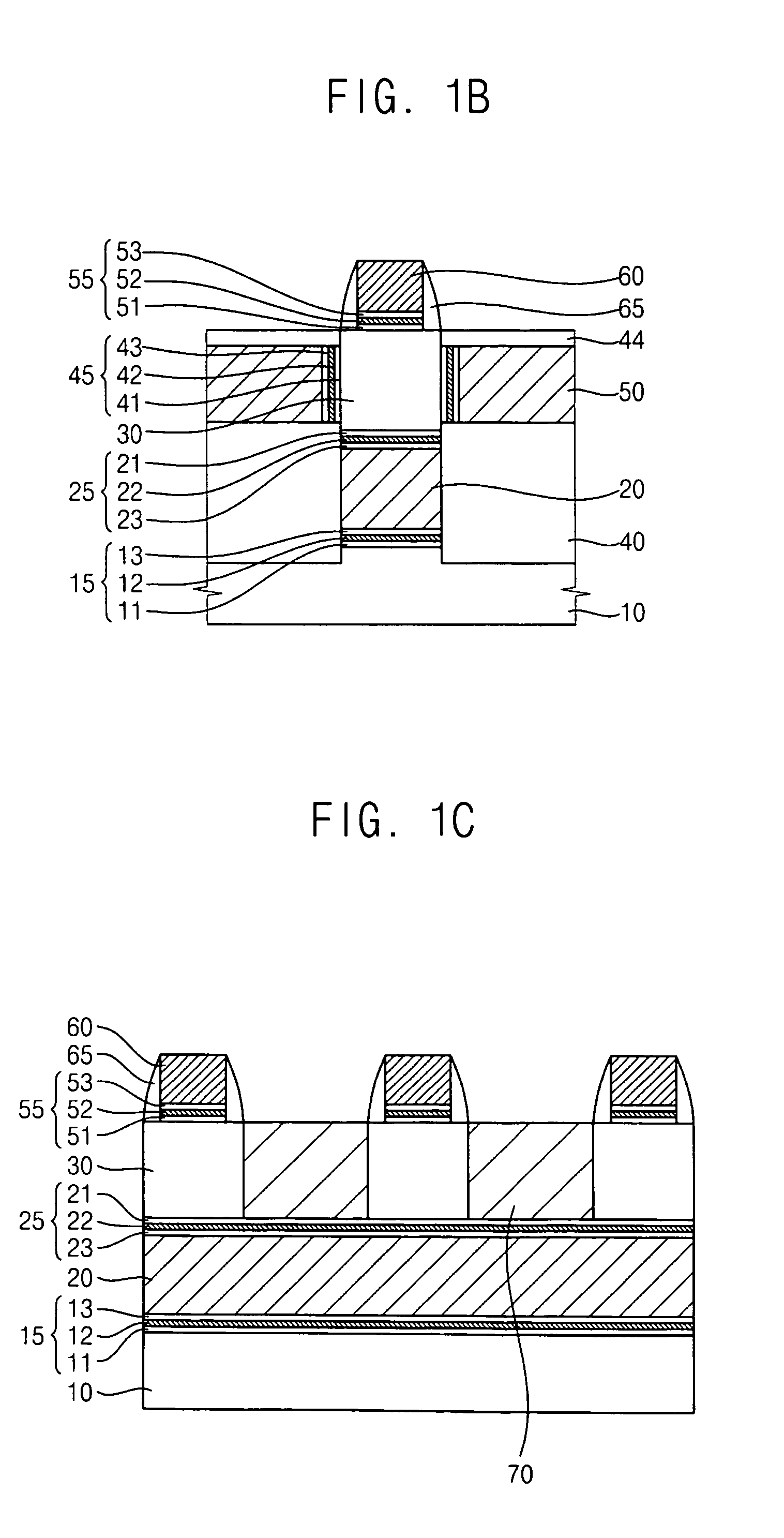
[0051]Detailed example embodiments are disclosed herein. However, specific structural and / or functional details disclosed herein are merely representative for purposes of describing example embodiments. The claims may, however, may be embodied in many alternate forms and should not be construed as limited to only example embodiments set forth herein.

[0052]It will be understood that when a component is referred to as being “on,”“connected to” or “coupled to” another component, it can be directly on, connected to or coupled to the other component or intervening components may be present. In contrast, when a component is referred to as being “directly on,”“directly connected to” or “directly coupled to” another component, there are no intervening components present. As used herein, the term “and / or” includes any and all combinations of one or more of the associated listed items.

[0053]It will be understood that, although the terms first, second, third, etc. may be used herein to describ...


PUM


Abstract

A example embodiment may provide a memory device that may include an active pattern on a semiconductor substrate, a first charge trapping layer pattern on the active pattern, a first gate electrode on the first charge trapping layer pattern, a second charge trapping layer pattern on a sidewall of the active pattern in a first direction, a second gate electrode on the second charge trapping layer pattern in the first direction, and / or a source / drain region in the active pattern. The memory device may have improved integration by forming a plurality of charge trapping layer patterns on the same active pattern.

Description

PRIORITY STATEMENT[0001]This application claims priority under 35 USC § 119 to Korean Patent Application No. 2006-102190 filed on Oct. 20, 2006, the contents of which are herein incorporated by reference in their entirety for all purposes.BACKGROUND[0002]1. Field[0003]Example embodiments relate to memory devices and methods of manufacturing the same. Example embodiments may relate, for example, to memory devices having improved integration and methods of manufacturing the same.[0004]2. Description of the Related Art[0005]Semiconductor memory devices may be classified into volatile memory devices such as dynamic random access memory (DRAM) devices or static random access memory (SRAM) devices, in which input / output operations of data may be performed relatively fast but data may be lost as time elapses, and non-volatile memory devices such as read only memory (ROM) devices, in which input / output operations of data may be performed relatively slow but data may be permanently stored.[0...

Claims


Application Information

Patent Timeline
Patent Type & Authority Patents(United States)
IPC IPC(8): H01L29/94H10B69/00
CPCH01L21/28282H01L27/115H01L27/11568H01L29/66833H01L29/7923H01L29/78648H01L29/40117H10B69/00H10B43/30
Inventor KIM, NA-YOUNGOH, CHANG-WOOKIM, SUNG-HWANCHOI, YONG-LACK
Owner SAMSUNG ELECTRONICS CO LTD
Features
  • R&D
  • Intellectual Property
  • Life Sciences
  • Materials
  • Tech Scout
  • Unparalleled Data Quality
  • Higher Quality Content
  • 60% Fewer Hallucinations
Learn More