Transfer substrate, transfer method, and organic electroluminescent device manufacturing method
a technology of transfer substrate and manufacturing method, which is applied in the direction of thermography, instruments, photosensitive materials, etc., can solve the problems of reducing luminescence efficiency and shortening brightness duration, and achieve the effect of long brightness duration and high luminescence efficiency
- Summary
- Abstract
- Description
- Claims
- Application Information
AI Technical Summary
Benefits of technology
Problems solved by technology
Method used
Image


Examples
example 1
a. Example 1
[0089]The blue luminescent device 41b configuring a display device is manufactured in the processes of 1 to 4.
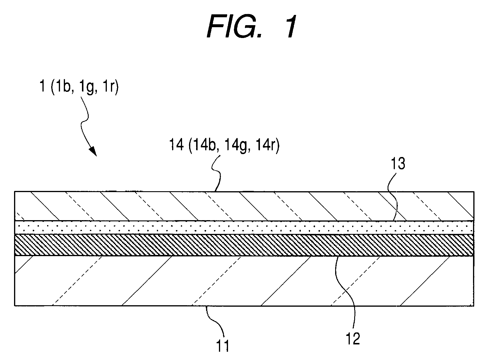
[0090]1. The transfer substrate 1b is manufactured as below. First of all, on the glass substrate (support substrate) 11, the light-to-heat conversion layer 12 is made by general sputtering using molybdenum (Mo) with the thickness of 200 nm. On the resulting light-to-heat conversion layer 12, the diffusion prevention layer 13 is formed by CVD using silicon nitride (SiNx) with the thickness of 100 nm. On the resulting diffusion prevention layer 13, the blue transfer layer 14b is formed by vacuum vapor deposition with a mixture of a host material being ADN with a blue luminescent guest material being DPAVBi with the weight percentage of 2.5.
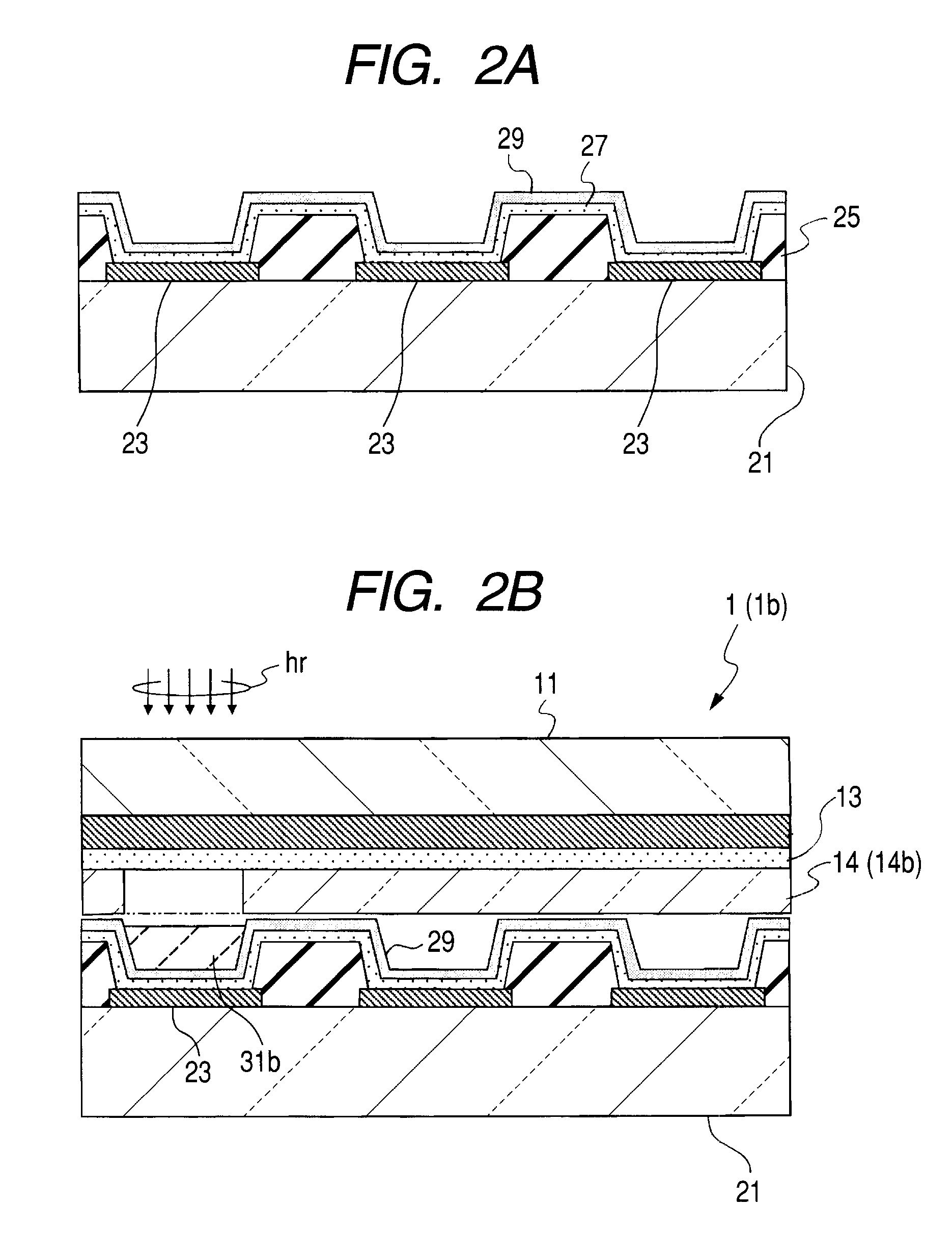
[0091]2. On the glass device 21 serving as a device substrate for device manufacturing, the lower electrode 23 is formed as an anode. The lower electrode 23 is of two-layer configuration, being a laminate of APC (Ag—Pd—Cu) layer...
example 2
[0094]In the procedure of manufacturing the transfer substrate 1b in the process 1 of Example 1, the blue luminescent device 41b is manufactured similarly to Example 1, except that the diffusion prevention layer 13 made of silicon oxide (SiO2) is formed on the light-to-heat conversion layer 12 by CVD with the thickness of 100 nm, and the blue transfer layer 14b is formed thereon.
example 3
[0096]In the procedure of manufacturing the transfer substrate 1b in the process 1 of Example 1, the green luminescent device 41g is manufactured similarly to Example 1, except for the material configuring the transfer layer.
[0097]That is, when the transfer substrate 1g is manufactured in the process 1, on the light-to-heat conversion layer 12 formed on the glass substrate 11, the diffusion prevention layer 13 made of silicon nitride (SiNx) is formed by CVD with the thickness of 100 nm. On thus formed diffusion prevention layer 13, the green transfer layer 14g is formed by vacuum vapor deposition with a mixture of a host material being ADN with a green luminescent guest material being coumarin 6 with the weight percentage of 5.
[0098]Using the transfer substrate manufactured as such, the green luminescent device 41g is manufactured with the procedure similar to the processes 2 to 4 of Example 1.
PUM
| Property | Measurement | Unit |
|---|---|---|
| wavelength | aaaaa | aaaaa |
| thickness | aaaaa | aaaaa |
| thickness | aaaaa | aaaaa |
Abstract
Description
Claims
Application Information
 - R&D
- Intellectual Property
- Life Sciences
- Materials
- Tech Scout
- Unparalleled Data Quality
- Higher Quality Content
- 60% Fewer Hallucinations
Browse by: Latest US Patents, China's latest patents, Technical Efficacy Thesaurus, Application Domain, Technology Topic, Popular Technical Reports.
© 2025 PatSnap. All rights reserved.Legal|Privacy policy|Modern Slavery Act Transparency Statement|Sitemap|About US| Contact US: help@patsnap.com