Supercharge Your Innovation With Domain-Expert AI Agents!

Display device and manufacturing method of the same

a technology of a display device and a manufacturing method, which is applied in the direction of semiconductor devices, instruments, electrical devices, etc., can solve the problems of lowering the ability to emit light and unstable quality of the semiconductor layer

Inactive Publication Date: 2009-07-07
SAMSUNG DISPLAY CO LTD
View PDF9 Cites 12 Cited by
  • Summary
  • Abstract
  • Description
  • Claims
  • Application Information

AI Technical Summary

Benefits of technology

The solution provides a stable display quality by compensating for semiconductor layer instability and light emission deterioration, maintaining effective light emission and image display over time.

Problems solved by technology

When the semiconductor layer made of the amorphous silicon is used for a long time, the quality of the semiconductor layer becomes unstable.
Also, an organic layer which generates light deteriorates if used for a long time, thereby lowering its ability to emit light.

Method used


Image

  • Display device and manufacturing method of the same
  • Display device and manufacturing method of the same
  • Display device and manufacturing method of the same

Examples


Embodiment Construction

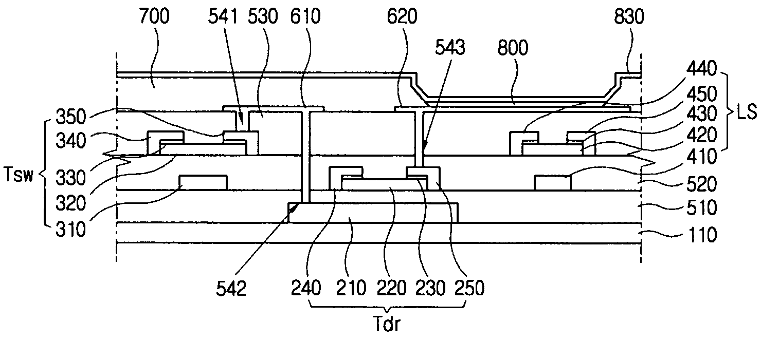
[0036]FIG. 1 illustrates an equivalent circuit of a display device according to a first exemplary embodiment of the present invention that includes a plurality of signal lines.

[0037]The signal lines include a gate line 911 which transmits a scanning signal, a negative electrode line 933 which supplies a negative voltage, a data line 922 which transmits a data signal, a voltage supply line 944 which transmits a driving voltage, and a sensor line 955 which is connected with a light sensor LS.

[0038]Each of pixels includes an organic light emitting element LD, a switching thin film transistor Tsw, a driving thin film transistor Tdr, a sensor thin film transistor Tss, the light sensor LS and capacitors C1 and C2.

[0039]The driving thin film transistor Tdr includes a control terminal, an input terminal, and an output terminal. The control terminal is connected with the switching thin film transistor Tsw. The input terminal is connected with the voltage supply line 944. The output terminal ...


PUM


Abstract

A display device according to the present invention comprises an insulating substrate; a switching thin film transistor formed on the insulating substrate for receiving a data voltage has a first semiconductor layer comprising amorphous silicon; a driving thin film transistor formed on the insulating substrate, having a control terminal connected with an output terminal of the switching thin film transistor and includes a second semiconductor layer comprising poly silicon; a light sensor formed on the insulating substrate and comprises a third semiconductor layer and a sensor input terminal and a sensor output terminal electrically connected with the third semiconductor layer; an insulating layer formed on the light sensor; a first electrode formed on the insulating layer and electrically connected with an output terminal of the driving thin film transistor; an organic layer formed on the first electrode and comprises a light emitting layer; a second electrode formed on the organic layer; and a controller which controls the data voltage based on an output of the light sensor.

Description

CROSS-REFERENCE TO RELATED APPLICATIONS[0001]This application claims priority from Korean Patent Application Nos. 2006-0011274, filed on Feb. 6, 2006, and 2006-0132948, filed on Dec. 22, 2006, in the Korean Intellectual Property Office, the disclosures of which are incorporated herein by reference.BACKGROUND OF THE INVENTION[0002]1. Field of the Invention[0003]This invention relates a display device and a method of manufacturing the same.[0004]2. Description of the Related Art[0005]Recently, the organic light emitting diode (OLED) has been of interest since it can be driven by a low voltage, is light and small, has a wide viewing angle, and has a high speed of response.[0006]The OLED typically has a plurality of thin film transistors per pixel.[0007]Generally, one pixel includes at least two thin film transistors, i.e., a switching transistor connected with a data line, and a driving transistor connected with a voltage supply line. The thin film transistors typically employ amorphou...

Claims


Application Information

Patent Timeline
Patent Type & Authority Patents(United States)
IPC IPC(8): H01L27/15
CPCG09G3/3225H01L27/3269G09G2300/0439G09G2300/0852H01L31/11G09G2360/148G09G2320/043H01L27/1229H10K59/13
Inventor KOH, BYUNG-SIKCHOI, JOON-HOOHUH, JONG-MOOGOH, JOON-CHULYOON, YOUNG-SOO
Owner SAMSUNG DISPLAY CO LTD
Features
  • R&D
  • Intellectual Property
  • Life Sciences
  • Materials
  • Tech Scout
  • Unparalleled Data Quality
  • Higher Quality Content
  • 60% Fewer Hallucinations
Learn More