Check patentability & draft patents in minutes with Patsnap Eureka AI!

Semiconductor memory device

a memory device and semiconductor technology, applied in the field of semiconductor memory devices, can solve the problems of reducing the service life of the memory cell, unable to charge the dummy bit line to a predetermined potential, and unable to ensure the timing margin of the desired timing, so as to achieve high-speed access and suppress the off leak current of the memory cell

Active Publication Date: 2009-12-29
PANASONIC SEMICON SOLUTIONS CO LTD
View PDF6 Cites 3 Cited by
  • Summary
  • Abstract
  • Description
  • Claims
  • Application Information

AI Technical Summary

Benefits of technology

[0014]An object of the present invention is to provide a semiconductor memory device capable of suppressing off leak current to ensure a timing margin or to prevent an access delay.
[0072]Thus, a semiconductor memory device of the present invention suppresses the off leak current of a dummy memory cell, thereby allowing a charge circuit to supply sufficient current to a dummy bit line so that the dummy bit line can be charged to a predetermined potential and a desired timing margin can be ensured.
[0073]Furthermore, another semiconductor memory device of the present invention suppresses the off leak current of a memory cell, thereby making it possible to realize a high speed access.

Problems solved by technology

However, in recent years, transistor off leak current has been significantly increased due to miniaturization in manufacturing technologies, and therefore, the conventional replica circuit presents a first problem as follows.
Since the conventional replica circuit utilizes the dummy bit line to which all the dummy memory cells are coupled, a current supplied from the charge circuit to the dummy bit line becomes insufficient, and thus it becomes impossible to charge the dummy bit line to a predetermined potential and to ensure a desired timing margin.
Furthermore, the conventional replica circuit presents a second problem as follows.
Due to memory cell off leak current, the charging of the bit line is delayed to cause an access delay, or data output of the sense amplifier becomes later than the timing generated by the replica circuit to cause an erroneous reading.

Method used


Image

  • Semiconductor memory device
  • Semiconductor memory device
  • Semiconductor memory device

Examples


Embodiment Construction

[0083]Hereinafter, embodiments of the present invention will be described with reference to the drawings.

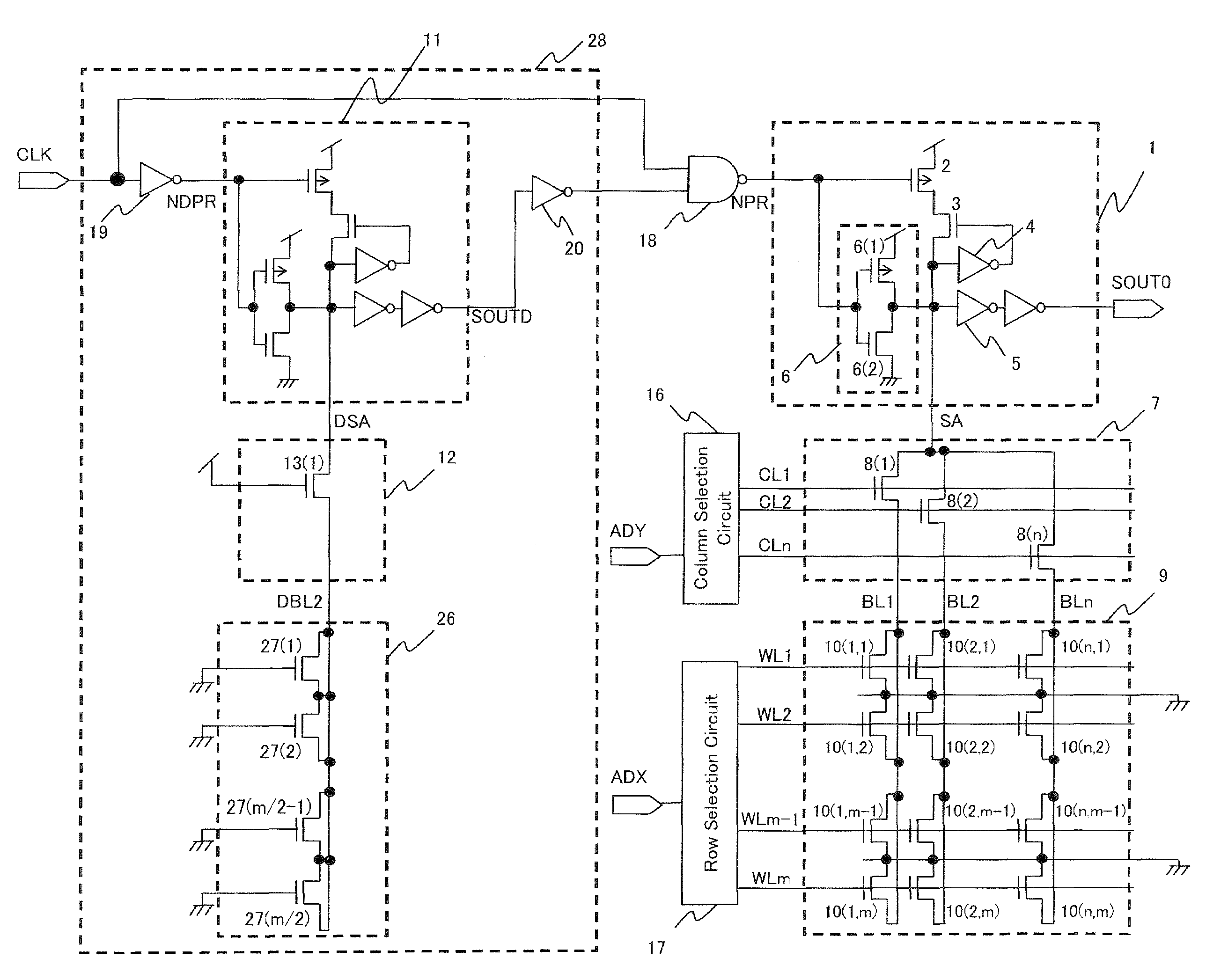
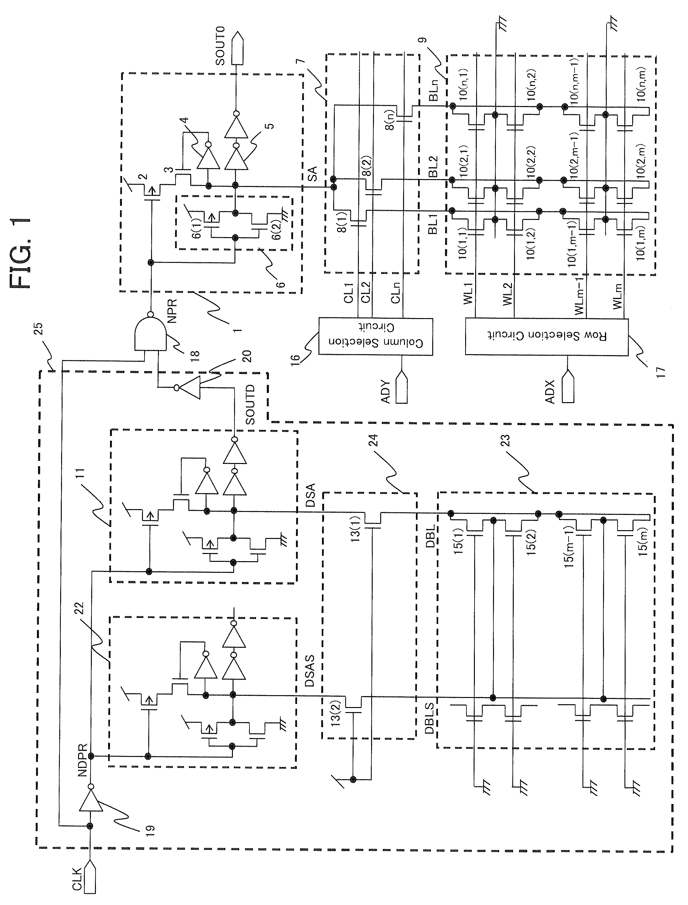
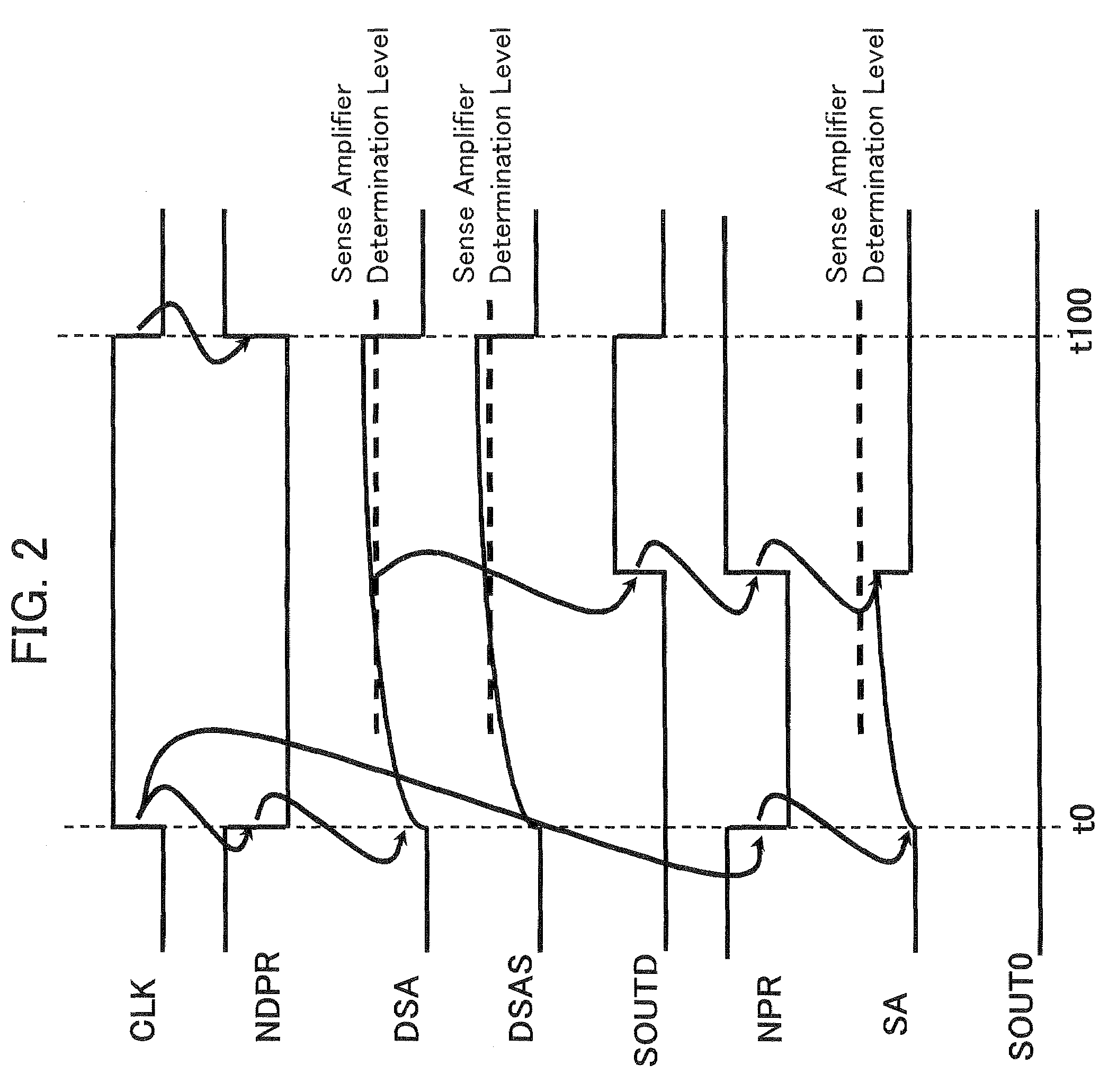
[0084]A semiconductor memory device according to Embodiment 1 of the present invention will be described with reference to FIG. 1. FIG. 1 is a circuit diagram showing a configuration of a read circuit of a mask ROM in Embodiment 1. In FIG. 1, the constituent elements denoted by the same reference characters as those in FIG. 8 function similarly, and therefore, only different constituent elements will be described below.

[0085]In a timing generation circuit 25, a dummy sense amplifier circuit 22 is configured similarly to a sense amplifier circuit 1. A dummy column gate 24 includes a transistor 13(1) and a transistor 13(2), gate inputs of which are coupled to a power supply, and which are configured similarly to those in a column gate 7. A dummy memory cell array 23 includes dummy memory cells 15(1) through 15(m), and sources of the dummy memory cells 15(1) through 15(m) are couple...


PUM


Abstract

In a conventional semiconductor memory device, a replica circuit configured by using a dummy bit line has been unable to charge the dummy bit line to a desired potential due to off leak current. Consequently, the time required for charging or discharging the dummy bit line differs from the desired time, and therefore, it has been unable to set optimum operation timing. To solve these problems, a semiconductor memory device of the present invention includes a dummy memory cell array in which source lines of dummy memory cells are charged simultaneously by a charge circuit configured similarly to a dummy bit line charge circuit, thus suppressing off leak current and performing appropriate timing generation.

Description

BACKGROUND OF THE INVENTION[0001]1. Field of the Invention[0002]The present invention relates to a semiconductor memory device such as a mask ROM.[0003]2. Prior Art[0004]A conventional semiconductor memory device such as a mask ROM utilizes, as a method for reducing current consumption, a replica circuit having a dummy sense amplifier circuit and a dummy memory cell circuit, which are configured similarly to a normal sense amplifier circuit and a normal memory cell circuit, in order to control an appropriate read operation time. Hereinafter, an operation method for a replica circuit in a conventional mask ROM will be described with reference to the drawings.[0005]FIG. 8 is a diagram showing a read circuit of a conventional mask ROM. A sense amplifier circuit 1 includes: a p-type transistor 2 whose gate input receives a pre-charge signal NPR; an n-type transistor 3 coupled in series to the p-type transistor 2; an inverter 4 whose input is coupled to a source node SA of the n-type tra...

Claims


Application Information

Patent Timeline
Patent Type & Authority Patents(United States)
IPC IPC(8): G11C8/00
CPCG11C7/12G11C16/28G11C16/24G11C7/14
Inventor KURATA, MASAKAZUHAYASHI, MITSUAKI
Owner PANASONIC SEMICON SOLUTIONS CO LTD
Features
  • R&D
  • Intellectual Property
  • Life Sciences
  • Materials
  • Tech Scout
  • Unparalleled Data Quality
  • Higher Quality Content
  • 60% Fewer Hallucinations
Learn More