Check patentability & draft patents in minutes with Patsnap Eureka AI!

Plastic microfabricated structure for biochip, microfabricated thermal device, microfabricated reactor, microfabricated reactor array, and micro array using the same

a micro-fabricated structure and biochip technology, applied in the direction of acceleration measurement using interia forces, laboratory glassware, instruments, etc., can solve the problems of difficult chamber application, difficult to remove thermal cross-talk, and increase the cost and time of fabrication, and achieve the effect of low cos

Active Publication Date: 2010-01-26
ELECTRONICS & TELECOMM RES INST
View PDF12 Cites 2 Cited by
  • Summary
  • Abstract
  • Description
  • Claims
  • Application Information

AI Technical Summary

Benefits of technology

[0010]The present invention is directed to a plastic microfabricated structure allowing micro patterns to be formed, and a microfabricated thermal device, a microfabricated reactor, a microfabricated reactor array and a micro array using the same, which may be fabricated by standard semiconductor process techniques and with a low cost compared to a conventional bio MEMS device employing conventional silicon or glass.

Problems solved by technology

When these techniques are employed, a thermal heater may be implemented for all reaction chambers, however, it is difficult to remove thermal cross-talk due to thermal isolation properties between reaction chambers.
Thus, it has a difficulty in applying for chambers which separately have an independent temperature circulation rule.
In addition, performance of devices is superior because they use a silicon material, however, it requires an extremely clean laboratory and high cost equipment capable of performing semiconductor processes, which causes fabrication cost and time to be increased, and makes it hard to apply for a single use medical diagnostic device.
However, this technique makes it hard to process the glass substrate and fabricate a heating thin layer having a small thermal mass.
As a result, power consumption is high and reaction speed is slow, which causes an additional Proportional Integrated Differential (PID) controller to be attached to.
Plastic in the lab-on-a-chip is significantly limited to be used for fabricating the structure such as fluid path, channel, and chamber among micro-fluidic devices.
Nevertheless, the plastic microfabricated structure could not have been applied for a thermal device of the lab-on-a-chip for the disease diagnosis due to a lack of technique for fabricating a structure having heat resistance, compatibility to semiconductor process technique, substrate flatness, and small thermal mass.

Method used


Image

  • Plastic microfabricated structure for biochip, microfabricated thermal device, microfabricated reactor, microfabricated reactor array, and micro array using the same
  • Plastic microfabricated structure for biochip, microfabricated thermal device, microfabricated reactor, microfabricated reactor array, and micro array using the same
  • Plastic microfabricated structure for biochip, microfabricated thermal device, microfabricated reactor, microfabricated reactor array, and micro array using the same

Examples


first embodiment

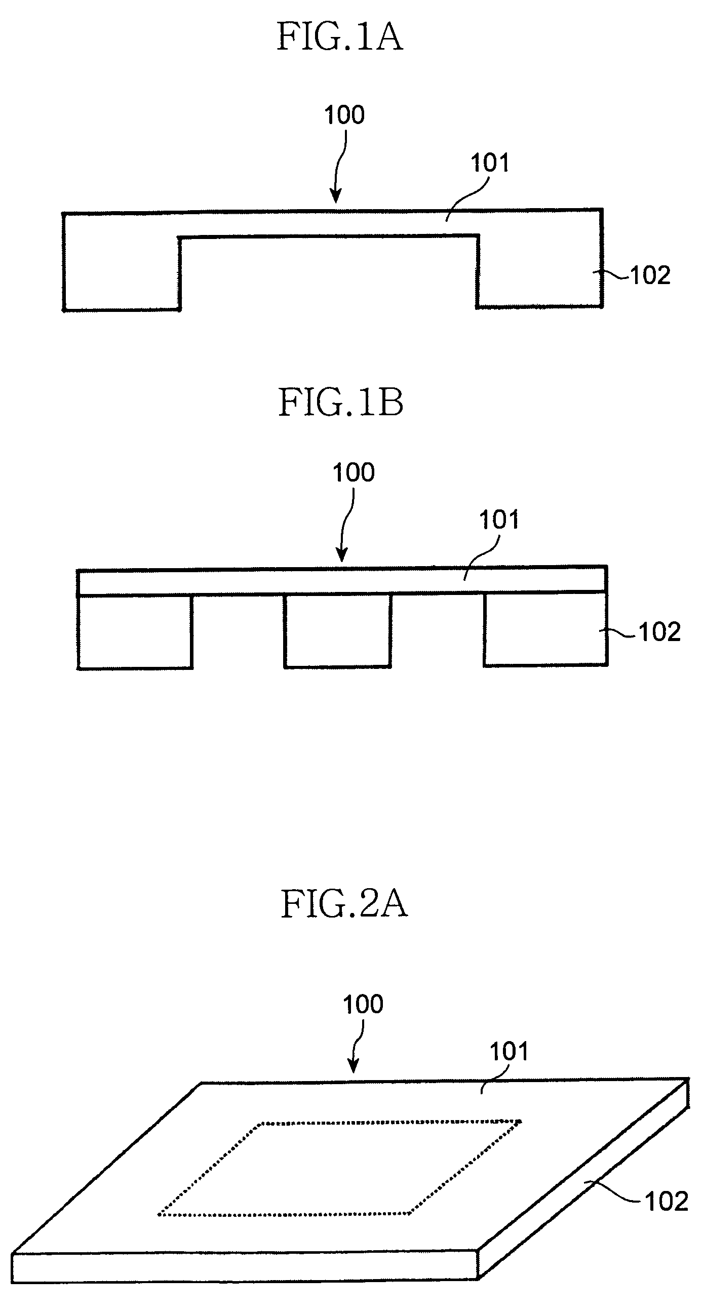
[0031]FIG. 1A and FIG. 1B are cross sectional views for explaining a plastic microfabricated structure in accordance with the present invention.

[0032]The plastic microfabricated structure of the present invention comprises a plastic microfabricated substrate 101 with its surface being flat for providing a heating region 100, and a support member 102 formed in a peripheral region of the heating region 100 to support the plastic microfabricated substrate 101.

[0033]The plastic microfabricated substrate 101 is formed of a material, which has a flatness (e.g., 0.1 nm˜500 nm) enough to apply a photolithography process, compatibility with respect to drug, a thin thinness of about 1 μm to 500 μm, slow heat conduction, and few thermal mass. The flatness of the plastic microfabricated substrate 101 should be enough to allow micro patterns of 0.01 μm in thickness and 1 μm in width to be formed on a typical wafer.

[0034]Examples of the plastic microfabricated substrate 101 may include a polymer ...

second embodiment

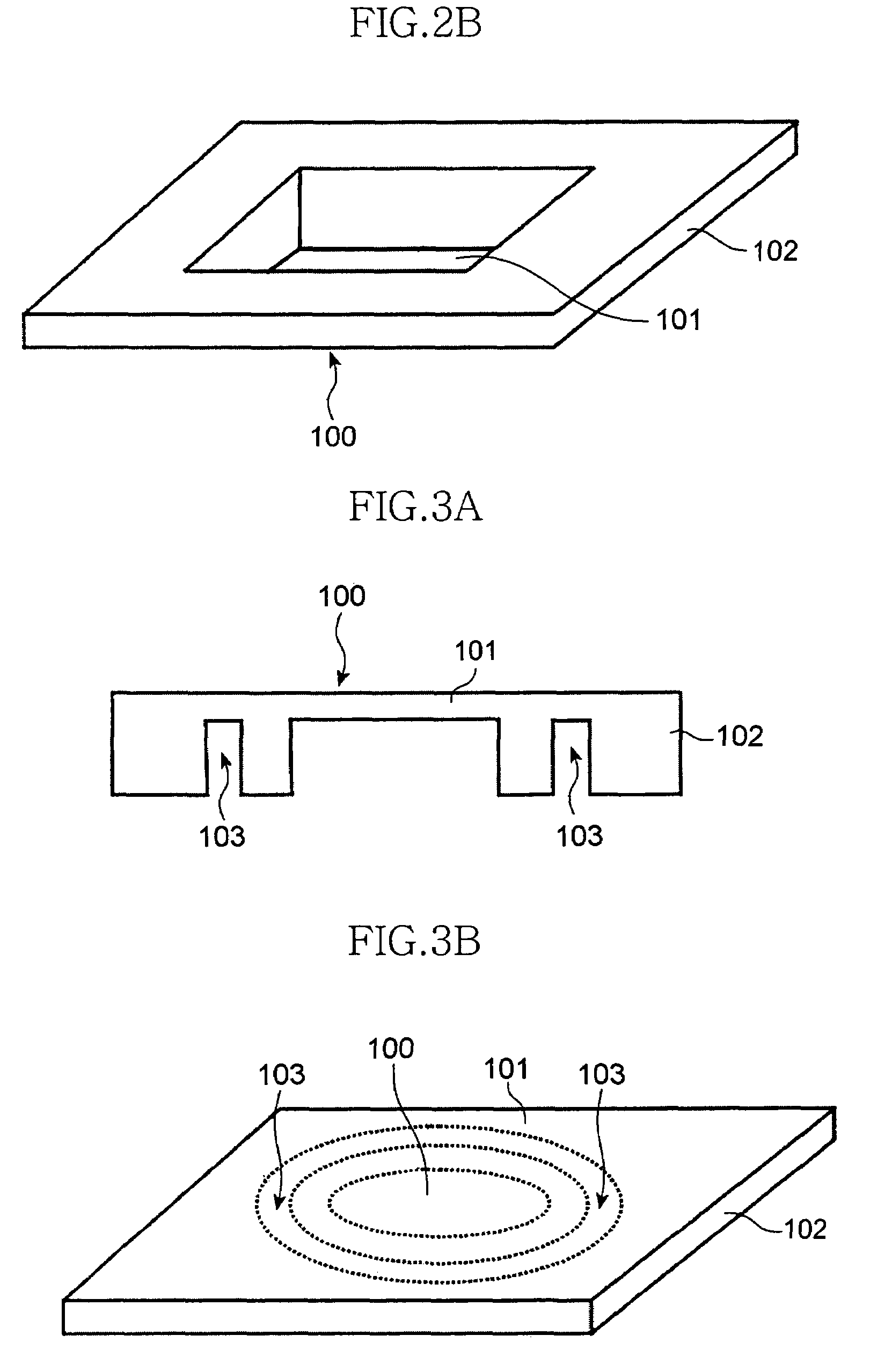
[0039]FIG. 3A and FIG. 3B are a cross sectional view and a perspective view for explaining a plastic microfabricated structure in accordance with the present invention, respectively.

[0040]These drawings are modified from the structure shown in FIG. 1A and FIG. 1B, wherein recesses 103 having a predetermined depth are formed around the heating region 100 of the bottom surface of the plastic microfabricated substrate 101. Alternatively, the recesses 103 may be circularly formed in the peripheral portion of the heating region 100.

[0041]By means of the recesses 103, thermal isolation of the heating region 100 may be enhanced when the plastic microfabricated structure of the present invention is used as a microfabricated thermal device, and the structure may be extended to any desired positions and to any degrees only with the single process when the structure is used for flow control.

third embodiment

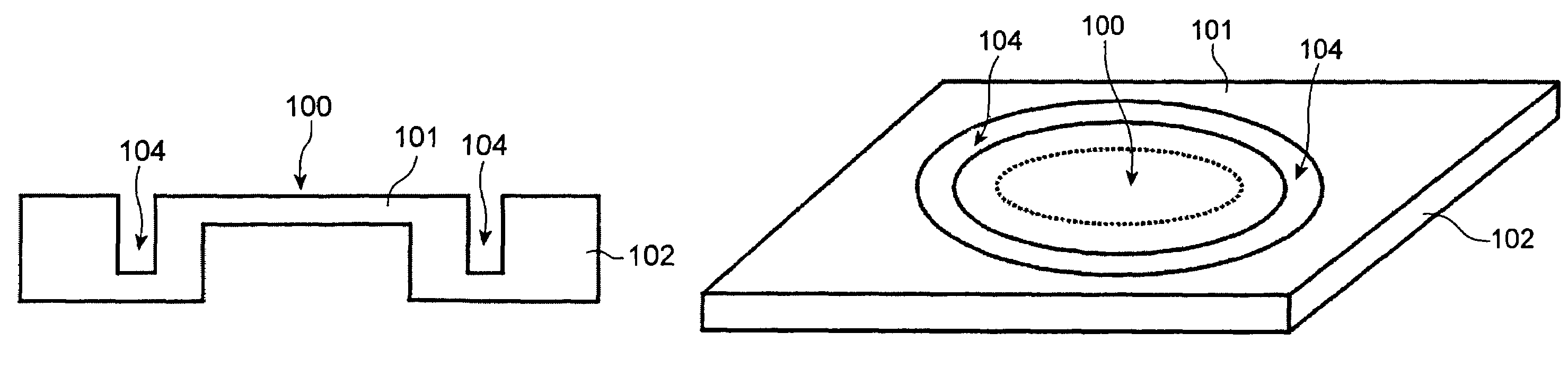
[0042]FIG. 4A and FIG. 4B are a cross sectional view and a perspective view for explaining a plastic microfabricated structure in accordance with the present invention, respectively.

[0043]These drawings are modified from the structure shown in FIG. 1A and FIG. 1B, wherein recesses 104 having a predetermined depth are formed around the heating region 100 of the front surface of the plastic microfabricated substrate 101. Alternatively, the recesses 104 may be circularly formed in the peripheral portion of the heating region 100.

[0044]By means of the recesses 104, thermal isolation of the heating region 100 may be enhanced when the plastic microfabricated structure of the present invention is used as a microfabricated thermal device, and the structure may be extended to any desired positions and to any degrees only with the single process when the structure is used for flow control. Alternatively, the recesses 104 may be used as a structure such as a flow path for flow control.


PUM

PropertyMeasurementUnit
thicknessaaaaaaaaaa
surface flatnessaaaaaaaaaa
temperatureaaaaaaaaaa

Abstract

Provided are a plastic microfabricated structure, and a microfabricated thermal device, a microfabricated reactor, a microfabricated reactor array and a micro array using the same, which may be applied to a bio chip, and the present invention may fabricate the plastic microfabricated structure for providing a heating region by means of insulating plastic, which has a thin thickness, flatness enough to allow a photolithography process to be performed, thermal isolation in its some or total area, and a small thermal mass, and on top of the heating region of the plastic microfabricated structure, a heater, a temperature sensor for sensing a temperature, an electrode, and an electrode pad are formed to thereby fabricate the microfabricated heating device, whereby element may be readily fabricated at a low cost, and the heating region is formed of a plastic thin layer, so that uniform temperature control is possible even with a low power, and various samples may be thermally treated at a fast speed to obtain their reaction and analysis.

Description

BACKGROUND[0001]1. Field of the Invention[0002]The present invention generally relates to a structure that may be used for micro reaction or analysis in a bio Micro Electro Mechanical System (MEMS), and more particularly, to a plastic microfabricated structure for a bio chip, and a microfabricated thermal device, a microfabricated reactor, a microfabricated reactor array and a micro array using the same, which employ plastic that has high flatness, thermal isolation, and small thermal mass.[0003]2. Discussion of Related Art[0004]In general, a bio MEMS device, in particular, a lab-on-a-chip for medical and disease diagnosis using DNA allows a real time diagnosis to be performed, so that many researches are conducted to implement its small size and low cost. Preference is made to general purpose medical diagnosis equipment such as single use type. As a result, attentions are moved from materials such as silicon and glass to plastics which require a relatively low cost in recent years....

Claims


Application Information

Patent Timeline
Patent Type & Authority Patents(United States)
IPC IPC(8): H01L29/06B01J19/00H01L23/02B01L3/00C40B60/14H01L23/10H01L27/14H01L29/82H01L29/84
CPCB01J19/0093B01L3/502707B01L3/50851B33Y80/00B01J2219/00605B01J2219/0061B01J2219/00619B01J2219/00621B01J2219/00635B01J2219/00637B01J2219/00659B01J2219/00783B01J2219/00804B01J2219/00833B01J2219/00853B01J2219/00858B01J2219/00873B01J2219/00961B01L2200/12B01L2200/147B01L2300/0819B01L2300/12B01L2300/1827C40B60/14B01J2219/00495H01L23/02
Inventor LEE, DAE SIKYANG, HAE SIKLIM, YONG TAIKCHUNG, KWANG HYOKIM, SUNG JINPARK, SE HOKIM, KYU WONKIM, YUN TAE
Owner ELECTRONICS & TELECOMM RES INST
Features
  • R&D
  • Intellectual Property
  • Life Sciences
  • Materials
  • Tech Scout
  • Unparalleled Data Quality
  • Higher Quality Content
  • 60% Fewer Hallucinations
Learn More